PLL103-02 View Datasheet(PDF) - Unspecified
Part Name
Description
Manufacturer
PLL103-02 Datasheet PDF : 7 Pages
| |||
PLL103-02
DDR SDRAM Buffer for Desktop PCs with 4 DDR DIMMS
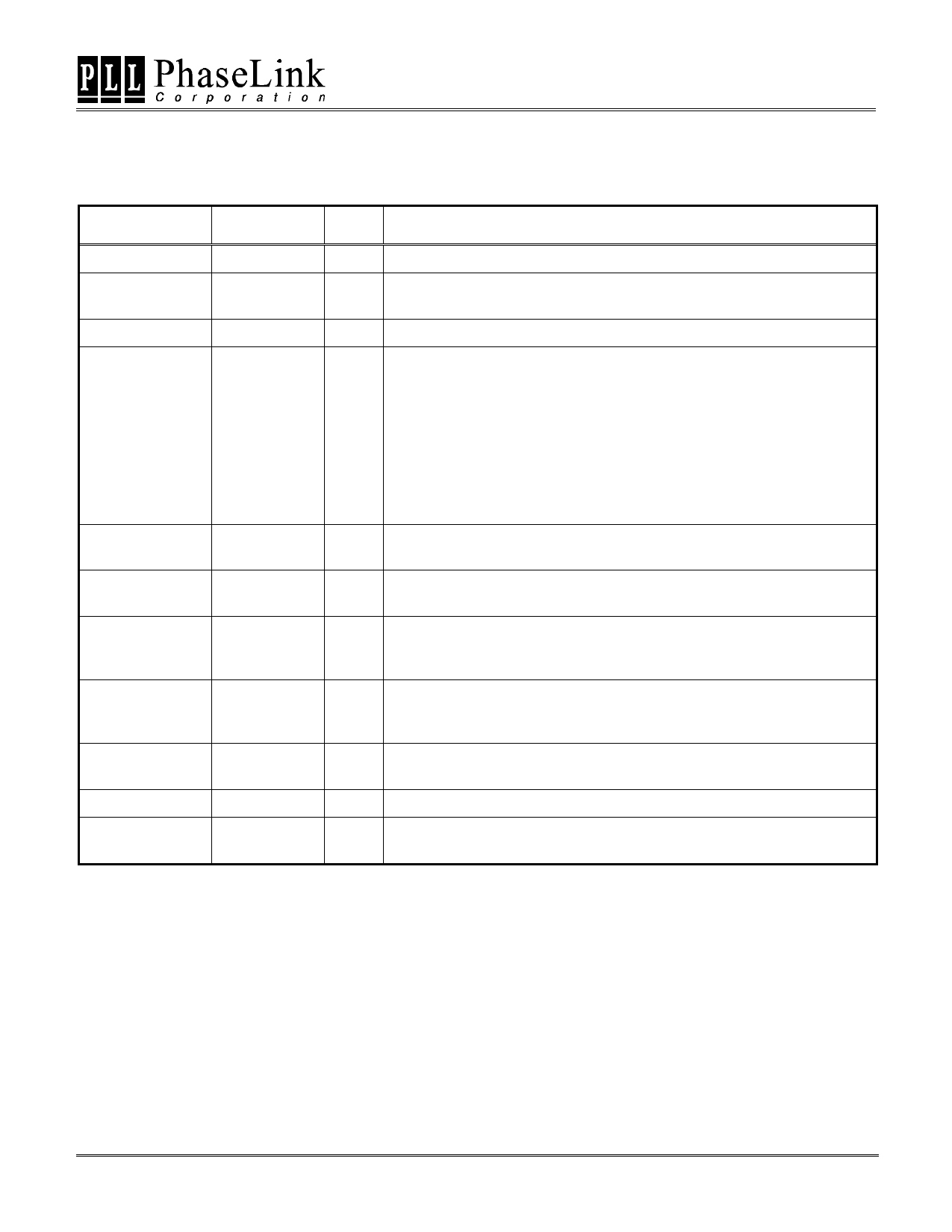
PIN DESCRIPTIONS
Name
Number Type
Description
FBOUT
1
O Feedback clock for chipset. Output voltage depends on VDD3.3_2.5V.
BUF_IN
13
I
Reference input from chipset. 3.3V input for STANDARD SDRAM mode;
2.5V input for DDR-ONLY mode.
PD
36
I Power Down Control input. When low, it will tri-state all outputs.
SEL_DDR
Input configure for DDR-ONLY mode or STANDARD SDRAM mode.
1 = DDR-ONLY mode (when VDD3.3_2.5 select 2.5V); 0 =
STANDARD SDRAM mode (when VDD3.3_2.5 select 3.3V). In
DDR-ONLY mode, pin 4, 5, 6, 7, 10, 11, 15, 16, 19, 20, 21, 22, 27,
48
I 28, 29, 30, 33, 34, 38, 39, 42, 43, 44 and 45 will be configured as
DDR outputs. In STANDARD SDRAM mode, pin 6, 7, 11, 15, 16, 19
and 20 will be configured as STANDARD SDRAM outputs. Pin 27,
28, 29, 30, 33, 34, 38, 39, 42, 43, 44 and 45 will be configured as
DDR outputs. Pin 4, 5, 21 and 22 will be Tri-stated.
DDR[0,5:11]T
4,21,28,30,34,
39,43,45
O
These outputs provide True copies of BUF_IN.
DDR[0,5:11]C
5,22,27,29,33,
38,42,44
O
These outputs provide complementary copies of BUF_IN.
DDR[1:4]T_SDRA
M [0,2,4,6]
6,10,15,19
When SEL_DDR=1, these outputs provide DDR mode outputs; when
O SEL_DDR=0, these outputs provide standard SDRAM mode outputs.
Voltage swing depends on VDD3.3_2.5.
DDR[1:4]C_SDRA
M [1,3,5,7]
7,11,16,20
When SEL_DDR=1, these outputs provide complementary copies of
O BUF_IN; when SEL_DDR=0, these outputs provide standard SDRAM
mode outputs. Voltage swing depends on VDD3.3_2.5.
VDD3.3_2.5
2,8,12,17,23
P
When VDD=2.5V, SEL_DDR=1. DDR-ONLY mode is selected; when
VDD=3.3V, SEL_DDR=0. STANDARD SDRAM mode is selected.
VDD2.5
32,37,41,47
P 2.5V power supply.
GND
3,9,14,18,26,
31,35,40,46
P Ground.
47745 Fremont Blvd., Fremont, California 94538 TEL (510) 492-0990 FAX (510) 492-0991
Rev 11/07/00 Page 2
Share Link: 