PSD913G3-C-90JI View Datasheet(PDF) - STMicroelectronics
Part Name
Description
Manufacturer
PSD913G3-C-90JI Datasheet PDF : 94 Pages
| |||
Preliminary Information
PSD9XX Family
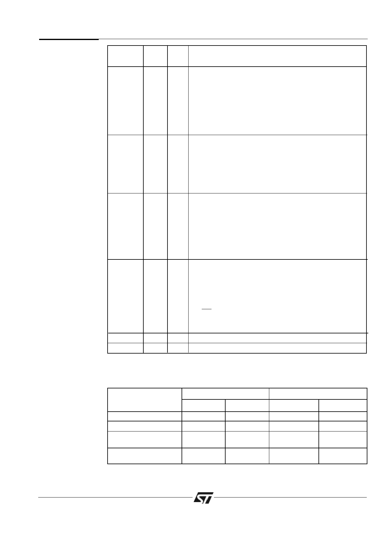
Table 5.
PSD9XX
Pin
Descriptions
(cont.)
Pin Name Pin* Type
(PLCC)
Description
PC7
PD0
PD1
PD2
VCC
GND
11 I/O
10 I/O
9
I/O
8
I/O
15, 38
1,16, 26
PC7 pin of Port C. This port pin can be configured to have
the following functions:
1. MCU I/O — write to or read from a standard output or
input port.
2. Input to the PLDs.
3. DBE — active-low Data Byte Enable input from 68HC912
type MCUs.
This pin can be configured as a CMOS or Open Drain output.
PD0 pin of Port D. This port pin can be configured to have
the following functions:
1. ALE/AS input latches address output from the MCU.
2. MCU I/O — write or read from a standard output or input
port.
3. Input to the PLDs.
4. General Purpose PLD output.
PD1 pin of Port D. This port pin can be configured to have
the following functions:
1. MCU I/O — write to or read from a standard output or
input port.
2. Input to the PLDs.
3. General Purpose PLD output
4. CLKIN — clock input to the automatic power-down
unit’s power-down counter, and the PLD AND array.
PD2 pin of Port D. This port pin can be configured to have
the following functions:
1. MCU I/O — write to or read from a standard output or
input port.
2. Input to the PLDs.
3. General Purpose PLD output.
4. CSI — chip select input. When low, the MCU can access
the PSD memory and I/O. When high, the PSD memory
blocks are disabled to conserve power.
Power pins
Ground pins
*The pin numbers in this table are for the PLCC package only. See the package information section for pin
numbers on other package types.
Table 6. I/O Port Latched Address Output Assignments*
Port A
Port B
Microcontroller
Port A (3:0) Port A (7:4) Port B (3:0) Port B (7:4)
8051XA (8-bit)
N/A
Address [7:4] Address [11:8] N/A
80C251 (page mode) N/A
N/A
Address [11:8] Address [15:12]
All other 8-bit
multiplexed
Address [3:0] Address [7:4] Address [3:0] Address [7:4]
8-bit non-multiplexed
bus
N/A
N/A
Address [3:0] Address [7:4]
N/A = Not Applicable
**Refer to the I/O Port Section on how to enable the Latched Address Output function.
13
Share Link: 