Q67007-A9399 View Datasheet(PDF) - Infineon Technologies
Part Name
Description
Manufacturer
Q67007-A9399 Datasheet PDF : 16 Pages
| |||
BTS 7710 G
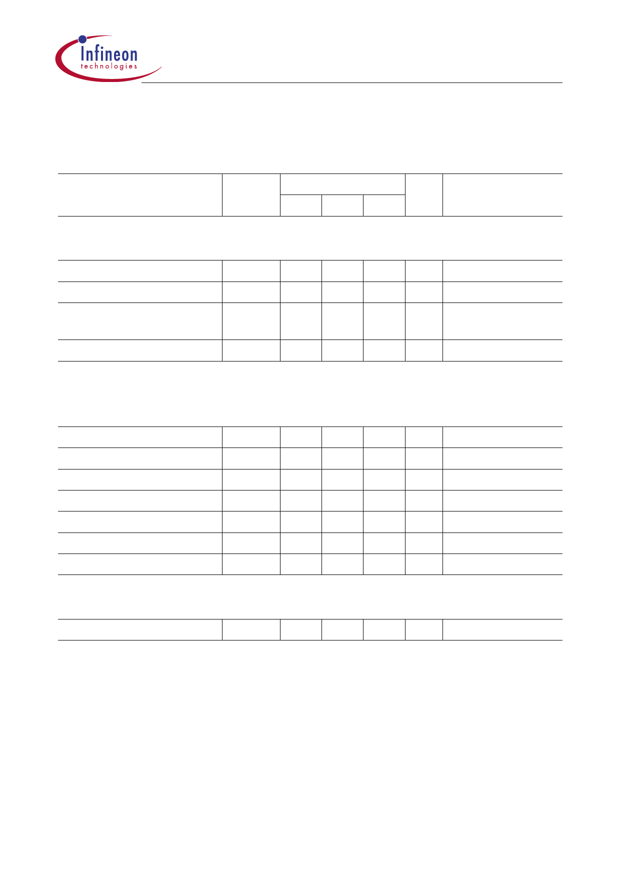
3.3 Electrical Characteristics (cont’d)
ISH1 = ISH2 = ISL1 = ISL2 = 0 A; – 40 C < Tj < 150 C; 8 V < VS < 18 V
unless otherwise specified
Parameter
Symbol Limit Values Unit Test Condition
min. typ. max.
Gate charge of lowside switch
Input to source charge;
QIS
–
4
6
nC ISL = 3 A; VS = 14 V
Input to drain charge;
QID
–
10 16 nC ISL = 3 A; VS = 14 V
Input charge total;
QI
–
28 43 nC ISL = 3 A; VS = 14 V
VIL = 0 to 10 V
Input plateau voltage;
V(plateau)
–
2.75 -
V
ISL = 3 A; VS = 14 V
Note: switching times and input charges are guaranteed by design
Control Inputs of highside switches IH 1, 2
H-input voltage
L-input voltage
Input voltage hysterese
H-input current
L-input current
Input series resistance
Zener limit voltage
VIH High
–
–
2.5 V –
VIH Low
1
–
–
V–
VIH HY
–
0.3 –
V–
IIH High
15
30
60
←A VGH = 5 V
IIH Low
5
–
20 ←A VGH = 0.4 V
RI
2.7 4
5.5 kτ –
VIH Z
5.4 –
–
V
IGH = 1.6 mA
Control Inputs IL1, 2
Gate-threshold-voltage
VIL th
0.9 1.7 2.2 V IDL = 1 mA
Note: The listed characteristics are ensured over the operating range of the integrated
circuit. Typical characteristics specify mean values expected over the production
spread. If not otherwise specified, typical characteristics apply at TA = 25 C and
the given supply voltage.
Data Sheet
12
2001-02-01
Share Link: 