Q67007-A9690 View Datasheet(PDF) - Infineon Technologies
Part Name
Description
Manufacturer
Q67007-A9690 Datasheet PDF : 21 Pages
| |||
TLE 7469
t
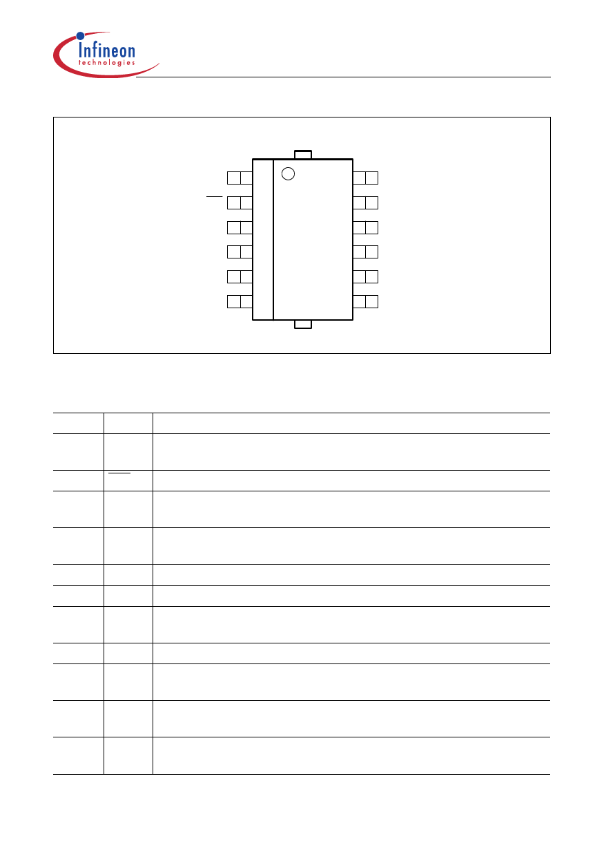
P-DSO-12-4
I1
1
IN H
2
Q1
3
SO
4
WDI
5
GND
6
12
I2
11
GND
10
Q2
9
RO
8
SI
7
DT
Figure 2
AEP03531.VS D
Pin Configuration (top view)
Table 1
Pin Definitions and Functions
Pin No. Symb. Function
1
I1
Input voltage 1; block to ground directly at the IC with a 100 nF
ceramic capacitor
2
INH Inhibit Input; low level disables the IC. Integrated pull-down resistor
3
Q1 Output voltage 1; 5.0 V, block to GND with a capacitor
CQ1 ≥ 1 µF, ESR < 6 Ω at 10 kHz
4
SO Sense output; Output of Early Warning Comparator, open collector
output
5
WDI Watchdog Input; Trigger Input for Watchdog pulses
6, 11 GND Ground; Pin 6, 11 and heat slug must be connected to GND
7
DT DT Delay timing; connect to GND, Q1 or Q2 to select Reset and
Watchdog timing
8
SI
Sense input; Input for Early Warning comparator
9
RO Reset output; open collector output with integrated 20 kΩ pull-up
resistor
10
Q2 Output voltage 2; 2.6 V (TLE 7469 GV52), 3.3 V (TLE 7469 GV53);
block to GND with a capacitor CQ2 ≥ 1 µF, ESR < 6 Ω at 10 kHz
12
I2
Input voltage 2; block to ground directly at the IC with a 100 nF
ceramic capacitor
Final Data Sheet
4
Rev. 1.3, 2004-10-28
Share Link: 