QT1101 View Datasheet(PDF) - Quantum Research Group
Part Name
Description
Manufacturer
QT1101 Datasheet PDF : 16 Pages
| |||
4 Specifications
4.1 Absolute Maximum Specifications
Operating temperature, Ta. . . . . . . . . . . . . . . . . . . . . . . . . . . . . . . . . . . . . . . . . . . . . . . . . . . . . . . . . . . . . . . . . . . . . . . . . . . . . . . . . . . . . . . . . . . . . . -40 ~ +85ºC
Storage temp, Ts. . . . . . . . . . . . . . . . . . . . . . . . . . . . . . . . . . . . . . . . . . . . . . . . . . . . . . . . . . . . . . . . . . . . . . . . . . . . . . . . . . . . . . . . . . . . . . . . . . . . . . -50 ~ +125ºC
Vdd. . . . . . . . . . . . . . . . . . . . . . . . . . . . . . . . . . . . . . . . . . . . . . . . . . . . . . . . . . . . . . . . . . . . . . . . . . . . . . . . . . . . . . . . . . . . . . . . . . . . . . . . . . . . . . . . . . . -0.3 ~ +6.0V
Max continuous pin current, any control or drive pin. . . . . . . . . . . . . . . . . . . . . . . . . . . . . . . . . . . . . . . . . . . . . . . . . . . . . . . . . . . . . . . . . . . . . . . . . . . . ±20mA
Short circuit duration to ground or Vdd, any pin. . . . . . . . . . . . . . . . . . . . . . . . . . . . . . . . . . . . . . . . . . . . . . . . . . . . . . . . . . . . . . . . . . . . . . . . . . . . . . . . . infinite
Voltage forced onto any pin. . . . . . . . . . . . . . . . . . . . . . . . . . . . . . . . . . . . . . . . . . . . . . . . . . . . . . . . . . . . . . . . . . . . . . . . . . . . . . . . . . -0.3V ~ (Vdd + 0.3) Volts
4.2 Recommended Operating Conditions
Operating temperature, Ta. . . . . . . . . . . . . . . . . . . . . . . . . . . . . . . . . . . . . . . . . . . . . . . . . . . . . . . . . . . . . . . . . . . . . . . . . . . . . . . . . . . . . . . . . . . . . . -40 ~ +85ºC
VDD. . . . . . . . . . . . . . . . . . . . . . . . . . . . . . . . . . . . . . . . . . . . . . . . . . . . . . . . . . . . . . . . . . . . . . . . . . . . . . . . . . . . . . . . . . . . . . . . . . . . . . . . . . . . . . . . . . . +2.8 ~ +5.0V
Short-term supply ripple+noise. . . . . . . . . . . . . . . . . . . . . . . . . . . . . . . . . . . . . . . . . . . . . . . . . . . . . . . . . . . . . . . . . . . . . . . . . . . . . . . . . . . . . . . . . . . . . . . ±5mV/s
Long-term supply stability. . . . . . . . . . . . . . . . . . . . . . . . . . . . . . . . . . . . . . . . . . . . . . . . . . . . . . . . . . . . . . . . . . . . . . . . . . . . . . . . . . . . . . . . . . . . . . . . . . . ±100mV
Cs range. . . . . . . . . . . . . . . . . . . . . . . . . . . . . . . . . . . . . . . . . . . . . . . . . . . . . . . . . . . . . . . . . . . . . . . . . . . . . . . . . . . . . . . . . . . . . . . . . . . . . . . . . . . . . . 2.2 ~ 100nF
Cx range. . . . . . . . . . . . . . . . . . . . . . . . . . . . . . . . . . . . . . . . . . . . . . . . . . . . . . . . . . . . . . . . . . . . . . . . . . . . . . . . . . . . . . . . . . . . . . . . . . . . . . . . . . . . . . . . . 0 ~ 50pF
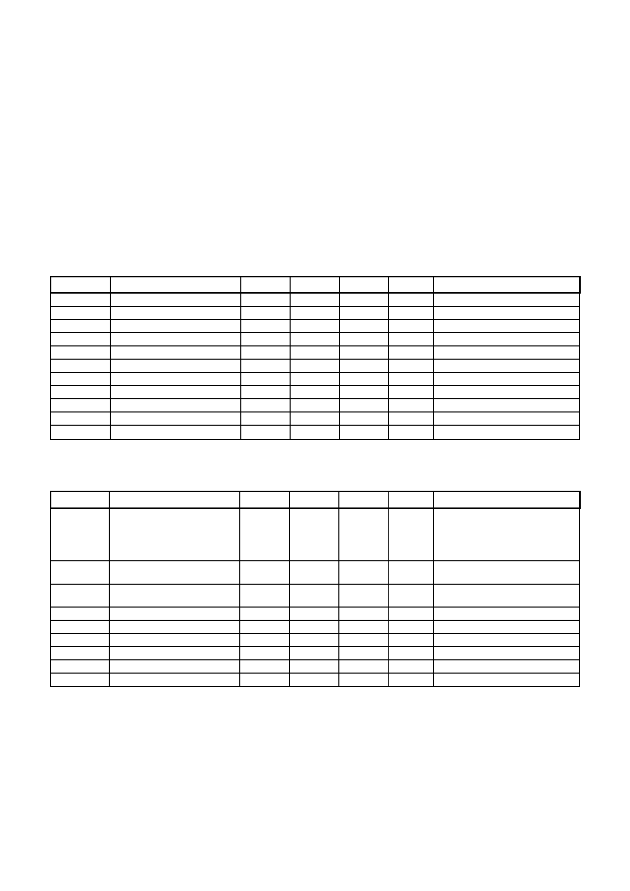
4.3 AC Specifications
Vdd = 5.0V, Ta = recommended, Cx = 5pF, Cs = 4.7nF; circuit of Figure 1.1
Parameter Description
Min
Typ
Max
Trc
Recalibration time
300
Fc
Burst center frequency
124
Fm
Burst modulation, percent
15
Tpc
Sample pulse duration
2
Tsu
Startup time from cold start
450
Tbd
Burst duration
6.5
Tdf
Response time - Fast mode
15
Tdn
Response time - normal mode
40
Tdl
Response time - LP mode
200
Tdr
Release time - all modes
40
bps
Serial communications speed
8,000
38,400
Units
ms
kHz
%
µs
ms
ms
ms
ms
ms
ms
baud
Notes
Total deviation
All 3 bursts
200ms LP setting
End of touch
4.4 DC Specifications
Vdd = 5.0V, Ta = recommended, Cx = 5pF, Cs = 4.7nF, Ta = recommended range; circuit of Figure 1.1 unless noted
Parameter Description
Min
Typ
Max
Units Notes
Iddn
Average supply current,
normal mode*
4.5
8
mA @ Vdd = 5.0
2.7
@ Vdd = 4.0
2.1
@ Vdd = 3.6
1.9
@ Vdd = 3.3
1.5
@ Vdd = 2.8
Iddl
Average supply current,
LP mode*
75
µA @ Vdd = 3.0; 200ms LP mode
Vdds
Average supply turn-on slope
100
V/s Req’d for startup, w/o external reset
ckt
Vil
Low input logic level
0.7
V
Vhl
High input logic level
3.5
V
Vol
Low output voltage
0.5
V
7mA sink
Voh
High output voltage
Vdd-0.5
V
2.5mA source
Iil
Input leakage current
±1
µA
Ar
Acquisition resolution
*No spread spectrum circuit
8
bits
Lq
10
QT1101 R4.06/0806
Share Link: 