QT118H-IG View Datasheet(PDF) - Quantum Research Group
Part Name
Description
Manufacturer
QT118H-IG Datasheet PDF : 14 Pages
| |||
1 - OVERVIEW
The QT118H is a digital burst mode charge-transfer (QT)
sensor designed specifically for touch controls; it includes all
hardware and signal processing functions necessary to
provide stable sensing under a wide variety of changing
conditions. Only a few low cost, non-critical discrete external
parts are required for operation.
Figure 1-1 shows the basic QT118H circuit using the device,
with a conventional output drive and power supply
connections. Figure 1-2 shows a second configuration using
a common power/signal rail which can be a long twisted pair
from a controller; this configuration uses the built-in pulse
mode to transmit the output state to the host controller.
1.1 BASIC OPERATION
The QT118H employs short, low duty cycle bursts of QT
cycles to acquire capacitance. Burst mode permits power
consumption in the low microamp range, dramatically
reduces RF emissions, lowers susceptibility to EMI, and yet
permits excellent response time. Internally the signals are
digitally processed to reject impulse noise, using a
'consensus' filter which requires four consecutive
confirmations of a detection before the output is activated.
The QT switches and charge measurement hardware
functions are all internal to the QT118H (Figure 1-3). A
single-slope switched capacitor ADC includes both the
required QT charge and transfer switches in a configuration
that provides direct ADC conversion. The sensitivity depends
on the values of Cs, Cx, and to a smaller degree, Vdd. Vdd is
used as the charge reference voltage.
Higher values of Cs increase gain; higher values of Cx load
reduce it. The value of Cs can thus be increased to allow
larger values of Cx to be tolerated (Figures 4-1 and 4-2, page
10).
Piezo sounder drive: The QT118H can drive a piezo
sounder after a detection for feedback. The piezo sounder
replaces or augments the Cs capacitor; this works since
piezo sounders are also capacitors, albeit with a large
thermal drift coefficient. If Cpiezo is in the proper range, no
additional capacitor. If Cpiezo is too small, it can simply be
‘topped up’ with a ceramic capacitor in parallel. The QT118H
drives a ~4kHz signal across SNS1 and SNS2 to make the
piezo (if installed) sound a short tone for 75ms immediately
after detection, to act as an audible confirmation.
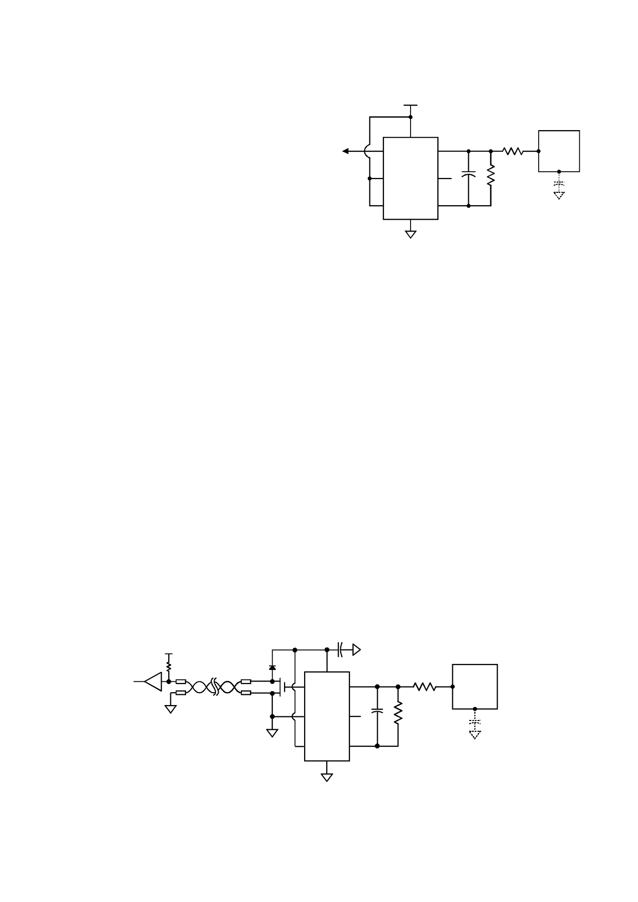
Figure 1-1 Standard mode options
+2.5 ~ +5
1
2
Vdd
7
RE
OUT
SNS2
3
OPT1
5
GAIN
Cs Rs
4
6
OPT2
SNS1
OUTPUT = DC
Vss
2nF - 500nF
TIMEOUT = 10 Secs
TOGGLE = OFF
8
GAIN = HIGH
SENSING
ELECTRODE
Cx
Option pins allow the selection or alteration of several special
features and sensitivity.
1.2 ELECTRODE DRIVE
The internal ADC treats Cs as a floating transfer capacitor; as
a direct result, the sense electrode can in theory be
connected to either SNS1 or SNS2 with no performance
difference. However, the noise immunity of the device is
improved by connecting the electrode to SNS2, preferably via
a series resistor Re (Figure 1-1) to roll off higher harmonic
frequencies, both outbound and inbound.
In order to reduce power consumption and to assist in
discharging Cs between acquisition bursts, a 470K series
resistor Rs should always be connected across Cs (Figure
1-1).
The rule Cs >> Cx must be observed for proper operation.
Normally Cx is on the order of 10pF or so, while Cs might be
10nF (10,000pF), or a ratio of about 1:1000.
It is important to minimize the amount of unnecessary stray
capacitance Cx, for example by minimizing trace lengths and
widths and backing off adjacent ground traces and planes so
as keep gain high for a given value of Cs, and to allow for a
larger sensing electrode size if so desired.
The PCB traces, wiring, and any components associated with
or in contact with SNS1 and SNS2 will become touch
sensitive and should be treated with caution to limit the touch
area to the desired location.
3.5 - 5.5V
CMOS
1K
LOGIC
Figure 1-2 2-wire operation, self-powered
+
Twisted
pair
1N4148
n-ch Mosfet
1 10µF
2
V dd
OUT SNS2
7
Cs
3 OPT1 GAIN 5
4 OPT2 SNS1 6
V ss
8
RE
Rs
SENSING
ELECTRODE
Cx
lq
2
QT118H R1.08 / 0405
Share Link: 