QT1080-IS48G View Datasheet(PDF) - Quantum Research Group
Part Name
Description
Manufacturer
QT1080-IS48G Datasheet PDF : 14 Pages
| |||
4 - SPECIFICATIONS
4.1 Absolute Maximum Specifications
Operating temperature, Ta. . . . . . . . . . . . . . . . . . . . . . . . . . . . . . . . . . . . . . . . . . . . . . . . . . . . . . . . . . . . . . . . . . . . . . . . . . . . . . . . . . . . . . . . . . . . . . -40 ~ +85ºC
Storage temp, Ts. . . . . . . . . . . . . . . . . . . . . . . . . . . . . . . . . . . . . . . . . . . . . . . . . . . . . . . . . . . . . . . . . . . . . . . . . . . . . . . . . . . . . . . . . . . . . . . . . . . -50ºC ~ +125ºC
Vdd. . . . . . . . . . . . . . . . . . . . . . . . . . . . . . . . . . . . . . . . . . . . . . . . . . . . . . . . . . . . . . . . . . . . . . . . . . . . . . . . . . . . . . . . . . . . . . . . . . . . . . . . . . . . . . . . . . . -0.3 ~ +6.0V
Max continuous pin current, any control or drive pin. . . . . . . . . . . . . . . . . . . . . . . . . . . . . . . . . . . . . . . . . . . . . . . . . . . . . . . . . . . . . . . . . . . . . . . . . . . . ±20mA
Short circuit duration to ground or Vdd, any pin. . . . . . . . . . . . . . . . . . . . . . . . . . . . . . . . . . . . . . . . . . . . . . . . . . . . . . . . . . . . . . . . . . . . . . . . . . . . . . . . . infinite
Voltage forced onto any pin. . . . . . . . . . . . . . . . . . . . . . . . . . . . . . . . . . . . . . . . . . . . . . . . . . . . . . . . . . . . . . . . . . . . . . . . . . . . . . . . . . -0.3V ~ (Vdd + 0.3) Volts
4.2 Recommended Operating Conditions
Operating temperature, Ta. . . . . . . . . . . . . . . . . . . . . . . . . . . . . . . . . . . . . . . . . . . . . . . . . . . . . . . . . . . . . . . . . . . . . . . . . . . . . . . . . . . . . . . . . . . . . . -40 ~ +85ºC
VDD. . . . . . . . . . . . . . . . . . . . . . . . . . . . . . . . . . . . . . . . . . . . . . . . . . . . . . . . . . . . . . . . . . . . . . . . . . . . . . . . . . . . . . . . . . . . . . . . . . . . . . . . . . . . . . . . . . . +2.8 ~ +5.0V
Short-term supply ripple+noise. . . . . . . . . . . . . . . . . . . . . . . . . . . . . . . . . . . . . . . . . . . . . . . . . . . . . . . . . . . . . . . . . . . . . . . . . . . . . . . . . . . . . . . . . . . . . . . ±5mV/s
Long-term supply stability. . . . . . . . . . . . . . . . . . . . . . . . . . . . . . . . . . . . . . . . . . . . . . . . . . . . . . . . . . . . . . . . . . . . . . . . . . . . . . . . . . . . . . . . . . . . . . . . . . . ±100mV
Cs range. . . . . . . . . . . . . . . . . . . . . . . . . . . . . . . . . . . . . . . . . . . . . . . . . . . . . . . . . . . . . . . . . . . . . . . . . . . . . . . . . . . . . . . . . . . . . . . . . . . . . . . . . . . . 2.2nF ~ 100nF
Cx range. . . . . . . . . . . . . . . . . . . . . . . . . . . . . . . . . . . . . . . . . . . . . . . . . . . . . . . . . . . . . . . . . . . . . . . . . . . . . . . . . . . . . . . . . . . . . . . . . . . . . . . . . . . . . . . . . 0 ~ 50pF
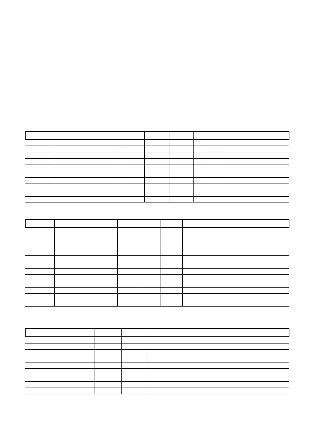
4.3 AC Specifications
Vdd = 5.0, Ta = recommended, Cx = 5pF, Cs = 4.7nF; circuit of Figure 1.1
Parameter Description
Min
Typ
Trc
Recalibration time
150
Fc
Burst center frequency
132
Fm
Burst modulation, percent
15
Tpc
Sample pulse duration
2
Tsu
Startup time from cold start
350
Tbd
Burst duration
3.4
Tdf
Response time - Fast mode
10
Tdn
Response time - Normal mode
25
Tdl
Response time - LP mode
200
Tdr
Release time - all modes
25
Max
Units
ms
kHz
%
µs
ms
ms
ms
ms
ms
ms
Notes
Total deviation
Both bursts together
200ms LP setting
End of touch
4.4 DC Specifications
Vdd = 5.0, Ta = recommended, Cx = 5pF, Cs = 4.7nF; circuit of Figure 1.1 unless noted
Parameter Description
Min
Typ
Max Units
IDDN
Supply current, normal mode*
4.5
8
mA
2.7
2.2
1.8
1.5
1.3
IDDL
Supply current, LP mode*
45
VDDS
Supply turn-on slope
100
VIL
Low input logic level
VHL
High input logic level
3.5
VOL
Low output voltage
VOH
High output voltage
Vdd-0.5
IIL
Input leakage current
AR
Acquisition resolution
8
*No spread spectrum circuit; Rosc = 18K ohms
µA
V/s
0.7
V
V
0.5
V
V
±1
µA
bits
Notes
@ Vdd = 5.0
@ Vdd = 4.0
@ Vdd = 3.6
@ Vdd = 3.3
@ Vdd = 3.0
@ Vdd = 2.8
@ Vdd = 3.0; 360ms LP mode
Req’d for startup, w/o external reset ckt
7mA sink
2.5mA source
4.5 Signal Processing
Vdd = 5.0, Ta = recommended, Cx = 5pF, Cs = 4.7nF
Description
Value
Units
Detection threshold
Detection hysteresis
Anti-detection threshold
Anti-detection recalibration delay
Detect Integrator filter, normal mode
Detect Integrator filter, ‘fast’ mode
Max On-Duration
10
2
6
2
6
2
10, 60, ∞
counts
counts
counts
secs
samples
samples
secs
Normal drift compensation rate
Anti drift compensation rate
2,000
500
ms/level
ms/level
Notes
Threshold for increase in Cx load
Threshold for decrease of Cx load
Time to recalibrate if Cx load has exceeded anti-detection threshold
Must be consecutive or detection fails
Must be consecutive or detection fails
Option pin selected
Towards increasing Cx load
Towards decreasing Cx load
lQ
9
QT1080 R11.03/0905
Share Link: 