RF3145PCBA-41X View Datasheet(PDF) - RF Micro Devices
Part Name
Description
Manufacturer
RF3145PCBA-41X Datasheet PDF : 18 Pages
| |||
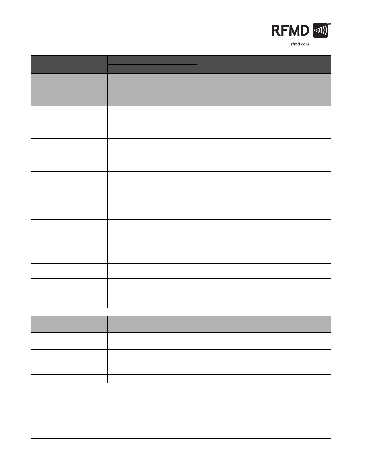
RF3145
Parameter
Specification
Min.
Typ.
Max.
GSM US 900MHz Band
Operating Frequency Range
Maximum Output Power
Total Efficiency (PAE)
Input Power for Max Output
Folding Conversion Gain
880
915
+34.5
+35.0
+32.5
0
45
55
35
+2
+4
+6
-5
Output Noise Power
Forward Isolation
Second Harmonic
Third Harmonic
All other Non-Harmonic Spurious
Cross Band Coupling 2F0
Input Impedance
Input VSWR
Output Load VSWR
Output Load Ruggedness
Output Load Impedance
Note: VRAMP,MAX=3/8*VBATT+0.18<1.6V
Power Control VRAMP,
GSM900 GMSK Mode
Power Control “ON”
Power Control “OFF”
Power Control Range
VRAMP Input Capacitance
VRAMP Input Current
Turn On/Off Time
-82
-86
50
6:1
10:1
50
-80
-84
-25
-5
-7
-36
-20
2.5:1
1.6
0.2
0.25
33
15
10
4
Unit
MHz
dBm
dBm
dBm
%
%
dBm
dB
dBm
dBm
dBm
dBm
dBm
dBm
dBm
Ω
Ω
Condition
Temp=+25 °C, VCC=3.5V,
BandSelect=Low, VMODE=Low,
VRAMP=VRAMP,MAX, PIN=+4dBm
Freq=880MHz to 915MHz, 25% Duty Cycle,
Pulse Width=1154μs, TX EN=High
Temp = 25°C, VCC=3.5V,
VRAMP= VRAMP,MAX
Temp=+85oC, VBATT=3.0V, VRAMP=VRAMP,MAX
VRAMP = 0.2 V
At POUT,MAX, VCC=3.5V
At POUT=31.5dBm
F0=915MHz, other signal 895MHz at -40dBm,
measured at 935MHz in 100kHz RBW (Max
Power)
RBW=100kHz, 925MHz to 935MHz,
POUT > +5 dBm
RBW=100kHz, 935MHz to 960MHz,
POUT > +5 dBm
TX_ENABLE=0V, VRAMP=0.2, PIN=+6dBm
Over all power levels
Over all power levels
Measured at DCS/PCS port. Over all power lev-
els.
Over all power levels
Spurious<-36dBm, VRAMP =0.2V to 1.6V,
RBW = 3 MHz
Load impedance presented at RF OUT pad
V
Max POUT, Voltage supplied to the input
V
Minimum POUT, Voltage supplied to the input.
dB
VRAMP=0.2V to 1.6V
pF
DC to 2MHz
μA
VRAMP = 1.6 V
μS
VRAMP=0V to 1.6V
4 of 18
7628 Thorndike Road, Greensboro, NC 27409-9421 · For sales or technical
support, contact RFMD at (+1) 336-678-5570 or sales-support@rfmd.com.
Rev A4 DS050919
Share Link: 