RJK5014DPK View Datasheet(PDF) - Renesas Electronics
Part Name
Description
Manufacturer
RJK5014DPK Datasheet PDF : 7 Pages
| |||
RJK5014DPK
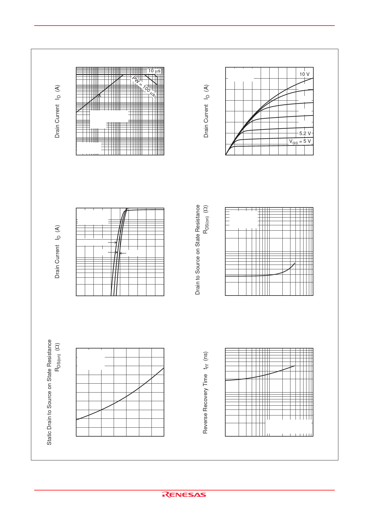
Main Characteristics
Maximum Safe Operation Area
100
10 μs
PW
10
= 100 μs
1
Operation in this
0.1
area is limited by
RDS(on)
0.01
Ta = 25°C
1 shot
0.001
0.1
1
10
100
1000
Drain to Source Voltage VDS (V)
Typical Transfer Characteristics
20
VDS = 10 V
10 Pulse Test
5
Tc = −25°C
2
25°C
1
75°C
0.5
0.2
0.1
0
2
4
6
8
10
Gate to Source Voltage VGS (V)
Static Drain to Source on State Resistance
vs. Temperature (Typical)
1
VGS = 10 V
ID = 8 A
0.8 Pulse Test
0.6
0.4
0.2
0
-25 0 25 50 75 100 125 150
Case Temperature Tc (°C)
REJ03G1458-0200 Rev.2.00 Oct 20, 2009
Page 3 of 6
Typical Output Characteristics
40
Ta = 25°C
Pulse Test
30
10 V
6V
5.8 V
20
5.6 V
5.4 V
10
5.2 V
VGS = 5 V
0
0
4
8
12 16 20
Drain to Source Voltage VDS (V)
Static Drain to Source on State Resistance
vs. Drain Current (Typical)
10
VGS = 10 V
Ta = 25°C
Pulse Test
1
0.1
1
10
100
Drain Current ID (A)
1000
Body-Drain Diode Reverse
Recovery Time (Typical)
100
di / dt = 100 A / μs
VGS = 0, Ta = 25°C
10
1
10
100
Reverse Drain Current IDR (A)
Share Link: 