RT8082 View Datasheet(PDF) - Richtek Technology
Part Name
Description
Manufacturer
RT8082 Datasheet PDF : 14 Pages
| |||
RT8082
Application Information
This IC is a single phase Buck PWM converter. It provides
single feedback loop, current mode control with fast
transient response. An internal 1V reference allows the
output voltage to be precisely regulated for low output
voltage applications. A fixed switching frequency (2MHz)
oscillator and internal compensation are integrated to
minimize external component count.
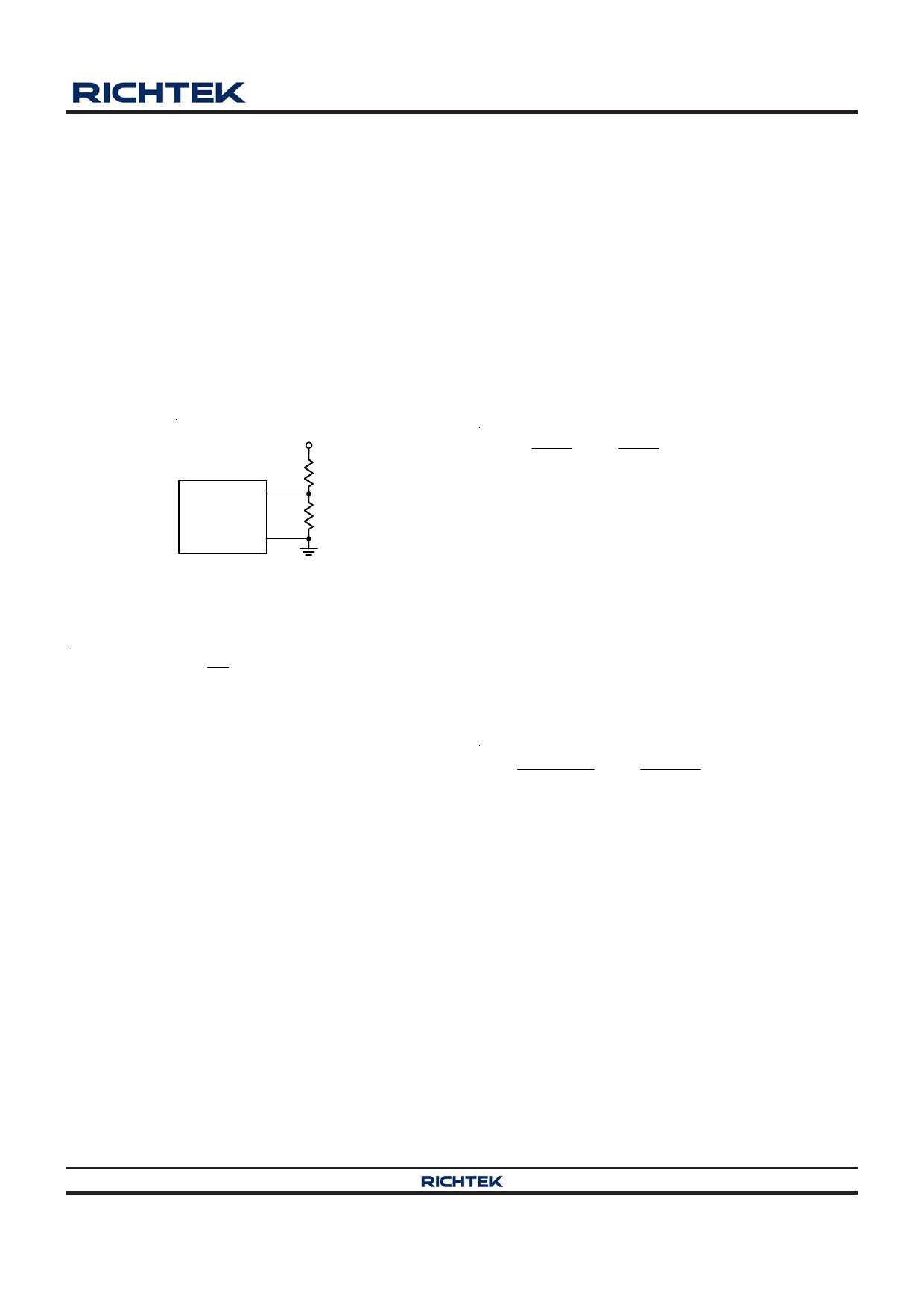
Output Voltage Setting
The resistive voltage divider allows the FB pin to sense
the output voltage as shown in Figure 1.
VOUT
R1
FB
RT8082
R2
AGND
Figure 1. Setting the Output Voltage
The output voltage is set by an external resistive voltage
divider according to the following equation :
VOUT
= VREF × ⎛⎜⎝1 +
R1
R2
⎞⎟⎠
where VREF is the feedback reference voltage (1V typ.).
Soft-Start
The IC contains an internal soft-start function to prevent
large inrush current and output voltage overshoot when
the converter is turned on. Soft-start automatically begins
once the chip's enable control is pulled to high. During
soft-start, the internal soft-start capacitor is charged and
generates a linear ramping-up voltage across the capacitor.
The VFB voltage tracks the internal ramping-up voltage
which will induce the duty pulse width to increase slowly
and in turn reduce the output surge current. Finally, the
internal 1V reference takes over the loop control once the
internal ramping-up voltage becomes higher than 1V. The
typical soft-start time is set at 1ms.
Power Good Output
The power good output is an open-drain output and requires
a pull up resistor. When the output voltage is 7% above or
7% below its set voltage, PGOOD will be pulled high. It is
held high until the output voltage returns within the allowed
tolerances once more. During soft-start, PGOOD is actively
held high and is only allowed to be low when soft-start
period is over and the output voltage reaches 93% of its
set voltage.
Inductor Selection
For a given input and output voltage, the inductor value
and operating frequency determine the ripple current. The
ripple current, ΔIL, increases with higher VIN and decreases
with higher inductance :
ΔIL
=
⎡ VOUT
⎢⎣ f ×L
⎤
⎥⎦
×
⎛⎝⎜1−
VOUT
VIN
⎞⎠⎟
Having a lower ripple current reduces not only the ESR
losses in the output capacitors but also the output voltage
ripple. High efficiency operation is achieved by reducing
ripple current at low frequency, but it requires a large
inductor to attain this goal.
For the ripple current selection, the value of ΔIL = 0.4(IMAX)
will be a reasonable starting point. The largest ripple current
occurs at the highest VIN. To guarantee that the ripple
current stays below a specified maximum, the inductor
value should be chosen according to the following
equation :
L=
⎡
⎢⎣
f
×
VOUT
ΔIL(MAX)
⎤
⎥⎦
×
⎛⎝⎜1−
VOUT
VIN(MAX)
⎞
⎠⎟
In this IC, 1μH is recommended for initial design. The
inductor's current rating (cause a 40°C temperature rising
from 25°C ambient) must be greater than the maximum
load current and ensure that the peak current will not
saturate the inductor during short circuit condition.
Input and Output Capacitors Selection
Higher value, lower cost ceramic capacitors are now
becoming available in smaller case sizes. Their high ripple
current, high voltage rating and low ESR make them ideal
for switching regulator applications. However, care must
be taken when these capacitors are used at the input and
output. When a ceramic capacitor is used at the input
and the power is supplied by a wall adapter through long
wires, a load step change at the output can induce ringing
Copyright ©2012 Richtek Technology Corporation. All rights reserved.
DS8082-00 November 2012
is a registered trademark of Richtek Technology Corporation.
www.richtek.com
11
Share Link: 