RT9001 View Datasheet(PDF) - Richtek Technology
Part Name
Description
Manufacturer
RT9001 Datasheet PDF : 9 Pages
| |||
RT9001
Absolute Maximum Ratings (Note 1)
z Supply Input Voltage -------------------------------------------------------------------------------------------------- 6.5V
z Power Dissipation, PD @ TA = 25°C
SOT-223 ----------------------------------------------------------------------------------------------------------------- 0.625W
z Package Thermal Resistance (Note 7)
SOT-223, θJA ------------------------------------------------------------------------------------------------------------ 160°C/W
z Lead Temperature (Soldering, 10 sec.) --------------------------------------------------------------------------- 260°C
z Junction Temperature ------------------------------------------------------------------------------------------------- 150°C
z Storage Temperature Range ---------------------------------------------------------------------------------------- – 65°C to 150°C
z ESD Susceptibility (Note 2)
HBM (Human Body Mode) ------------------------------------------------------------------------------------------ 2kV
MM (Machine Mode) -------------------------------------------------------------------------------------------------- 200V
Recommended Operating Conditions (Note 3)
z Supply Input Voltage -------------------------------------------------------------------------------------------------- 2.8V to 5.5V
z Junction Temperature Range ---------------------------------------------------------------------------------------- – 40°C to 125°C
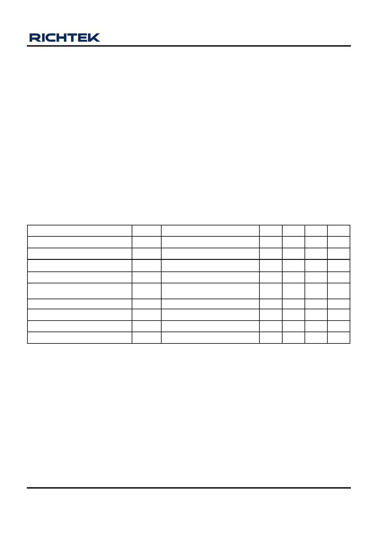
Electrical Characteristics
(VIN = VOUT + 1V or VIN = 2.8V whichever is greater, CIN = 1μF, COUT = 1μF, TA = 25° C, unless otherwise specified)
Parameter
Symbol
Test Conditions
Min Typ Max
Units
Output Voltage Accuracy
ΔVOUT IOUT = 1mA
−1
--
+3
%
Current Limit
ILIM
RLOAD = 1Ω
600 --
-- mA
Quiescent Current (Note 6)
IQ
IOUT = 0mA
-- 220 300 μA
Dropout Voltage (Note 4)
Line Regulation
Load Regulation (Note 5)
Power Supply Rejection Rate
VDROP
ΔVLINE
ΔVLOAD
PSRR
IOUT = 600mA
VIN = (VOUT + 0.3V) to 5.5V,
IOUT = 1mA
1mA < IOUT < 600mA
f = 1kHz, COUT = 1μF
-- 580 -- mV
-- 0.2 -- %/V
--
30 55 mV
--
−55 --
dB
Thermal Shutdown Temperature TSD
-- 170 --
°C
Thermal Shutdown Hysteresis
ΔTSD
--
40
--
°C
Note 1. Stresses listed as the above “Absolute Maximum Ratings” may cause permanent damage to the device. These are for
stress ratings. Functional operation of the device at these or any other conditions beyond those indicated in the
operational sections of the specifications is not implied. Exposure to absolute maximum rating conditions for extended
periods may remain possibility to affect device reliability.
Note 2. Devices are ESD sensitive. Handling precaution recommended.
Note 3. The device is not guaranteed to function outside its operating conditions.
Note 4.The dropout voltage is defined as VIN -VOUT, which is measured when VOUT is VOUT(NORMAL) − 100mV.
Note 5. Regulation is measured at constant junction temperature by using a 20ms current pulse. Devices are tested for load
regulation in the load range from 1mA to 600mA respectively.
Note 6. Quiescent, or ground current, is the difference between input and output currents. It is defined by IQ = IIN - IOUT under
no load condition (IOUT = 0mA). The total current drawn from the supply is the sum of the load current plus the ground
pin current.
Note 7. θJA is measured in the natural convection at TA = 25°C on a low effective thermal conductivity test board of
JEDEC 51-3 thermal measurement standard.
DS9001-04 March 2007
www.richtek.com
3
Share Link: 