RT9016 View Datasheet(PDF) - Richtek Technology
Part Name
Description
Manufacturer
RT9016 Datasheet PDF : 11 Pages
| |||
RT9016
Preliminary
Applications Information
Like any low-dropout regulator, the external capacitors used
with the RT9016 must be carefully selected for regulator
stability and performance. Using a capacitor whose value
is > 1μF on the RT9016 input and the amount of
capacitance can be increased without limit. The input
capacitor must be located a distance of not more than
0.5 inch from the input pin of the IC and returned to a
clean analog ground. Any good quality ceramic or
tantalum can be used for this capacitor. The capacitor
with larger value and lower ESR (equivalent series
resistance) provides better PSRR and line-transient
response. The output capacitor must meet both
requirements for minimum amount of capacitance and
ESR in all LDOs application. The RT9016 is designed
specifically to work with low ESR ceramic output capacitor
in space-saving and performance consideration. Using
a ceramic capacitor whose value is at least 1μF with ESR
is > 25mΩ on the RT9016 output ensures stability. The
RT9016 still works well with output capacitor of other types
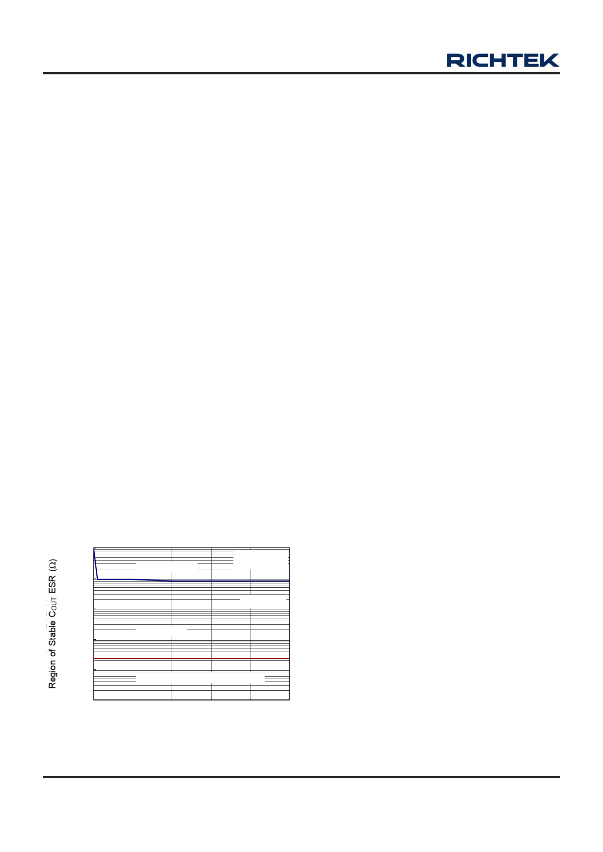
due to the wide stable ESR range. Figure 1 shows the
curves of allowable ESR range as a function of load current
for various output capacitor values. Output capacitor of
larger capacitance can reduce noise and improve load
transient response, stability, and PSRR. The output
capacitor should be located not more than 0.5 inch from
the VOUT pin of the RT9016 and returned to a clean analog
ground.
Region of Stable COUT ESR vs. Load Current
1001.0000
RT9016-15PB
Unstable Region
CIN = 1μF, X7R
10.0100
1.001
COUT = 1uF
Stable Region
0.10
0.01
0.00
0
Unstable Region (Simulation Verity)
100
200
300
400
500
Load Current (mA)
Figure 1
Bypass Capacitor and Low Noise
Connecting a 22nF between the BP pin and GND pin
significantly reduces noise on the regulator output, it is
critical that the capacitor connection between the BP pin
and GND pin be direct and PCB traces should be as short
as possible. There is a relationship between the bypass
capacitor value and the LDO regulator turn on time. DC
leakage on this pin can affect the LDO regulator output
noise and voltage regulation performance.
Enable Function
The RT9016 features an LDO regulator enable/disable
function. To assure the LDO regulator will switch on, the
EN turn on control level must be greater than 1.2 volts.
The LDO regulator will go into the shutdown mode when
the voltage on the EN pin falls below 0.4 volts. For to
protecting the system, the RT9016 have a quick-discharge
function. If the enable function is not needed in a specific
application, it may be tied to VIN to keep the LDO regulator
in a continuously on state.
Thermal Considerations
Thermal protection limits power dissipation in RT9016.
When the operation junction temperature exceeds 165°C,
the OTP circuit starts the thermal shutdown function turn
the pass element off. The pass element turn on again
after the junction temperature cools by 30°C.
RT9016 lowers its OTP trip level from 165°C to 110°C
when output short circuit occurs (VOUT < 0.4V) as shown
in Figure 2. This limits IC case temperature under 100°C
and provides maximum safety to end users when output
short circuit occurs.
For continue operation, do not exceed absolute maximum
operation junction temperature 125°C. The power
dissipation definition in device is :
PD = (VIN−VOUT) x IOUT + VIN x IQ
The maximum power dissipation depends on the thermal
resistance of IC package, PCB layout, the rate of
surroundings airflow and temperature difference between
junction to ambient. The maximum power dissipation can
be calculated by following formula :
www.richtek.com
8
DS9016-03 August 2007
Share Link: 