LC378100QM View Datasheet(PDF) - SANYO -> Panasonic
Part Name
Description
Manufacturer
LC378100QM Datasheet PDF : 4 Pages
| |||
LC378100QM, QT
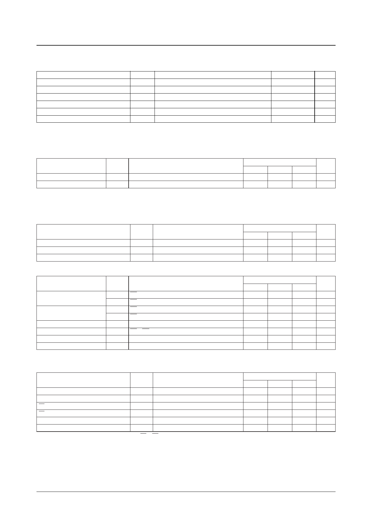
Specifications
Absolute Maximum Ratings *1
Parameter
Symbol
Conditions
Ratings
Unit
Supply voltage
Supply input voltage
Supply output voltage
Allowable power dissipation
VCC
ã0.3 to +7.0
V
VIN
ã0.3*2 to VCC + 0.3
V
VOUT
ã0.3 to VCC + 0.3
V
Pd max Ta = 25ô¯C; Reference values for the SANYO DIP package
1.0
W
Operating temperature
Topr
ã10 to +70
ô¯C
Storage temperature
Tstg
ã55 to +125
ô¯C
Note: 1. Permanent device damage may occur if Absolute Maximum Ratings are exceeded. Functional operation should be restricted to Recommended
Operating Conditions.
2. VIN (min) = ã3.0 V (pulse width ãÊ 30 ns)
Input/Output Capacitance* at Ta = 25ô¯C, f = 1.0 MHz
Parameter
Symbol
Conditions
Input capacitance
CIN
VIN = 0 V; Reference values for the SANYO DIP package
Output capacitance
COUT VOUT = 0 V; Reference values for the SANYO DIP package
Note: * This parameter is periodically sampled and not 100% tested.
Ratings
Unit
min
typ
max
8
pF
10
pF
DC Recommended Operating Ranges at Ta = ã10 to +70ô¯C, VCC = 2.6 to 5.5 V
Parameter
Symbol
Conditions
Supply voltage
VCC
Input high level voltage
VIH
Input low level voltage
VIL
DC Electrical Characteristics at Ta = ã10 to +70ô¯C, VCC = 2.6 to 5.5 V
Ratings
Unit
min
typ
max
2.6
5.0
5.5
V
2.2
ã0.3
VCC + 0.3
V
+0.6
V
Parameter
Symbol
Conditions
Operating supply current
Standby supply current
Input leakage current
Output leakage current
Output high level voltage
Output low level voltage
Note: * Guaranteed at Ta = 25ô¯C
ICCA1
ICCA2
ICCS1
ICCS2
ILI
ILO
VOH
VOL
CE = 0.2 V, VI = VCC ã 0.2 V/0.2 V
CE = VIL, IO = 0 mA, VI = VIH/VIL, f = 10 MHz
CE = VCC ã 0.2 V
CE = VIH
VIN = 0 to VCC
CE or OE = VIH, VOUT = 0 to VCC
IOH = ã0.5 mA
IOL = 0.5 mA
min
0.8 VCC
Ratings
typ
max
30
55
30 (1.0)
1.0 (300)
ôÝ1.0
ôÝ1.0
0.2
Unit
mA
mA
ôçA
mA(ôçA)
ôçA
ôçA
V
V
AC Characteristics at Ta = ã10 to +70ô¯C, VCC = 2.6 to 5.5 V
Parameter
Symbol
Conditions
Cycle time
tCYC
Address access time
tAA
CE access time
tCA
OE access time
tOA
Output hold time
tOH
Output disable time*1
tOD*1
Note: 1. tOD is measured from the earlier edge of the CE or OEãs going high impedance.
This parameter is periodically sampled and not 100% tested.
2. Guaranteed at VCC = 4.5 to 5.5 V
min
200 (120)
Ratings
typ
20
Unit
max
ns
200 (120) ns
200 (100) ns
80 (40) ns
ns
100 ns
No. 5611-3/4
Share Link: 