S3C8285 View Datasheet(PDF) - Samsung
Part Name
Description
Manufacturer
S3C8285 Datasheet PDF : 369 Pages
| |||
REVISION DESCRIPTIONS
1. CHAPTHER 20 ELECTRICAL DATA
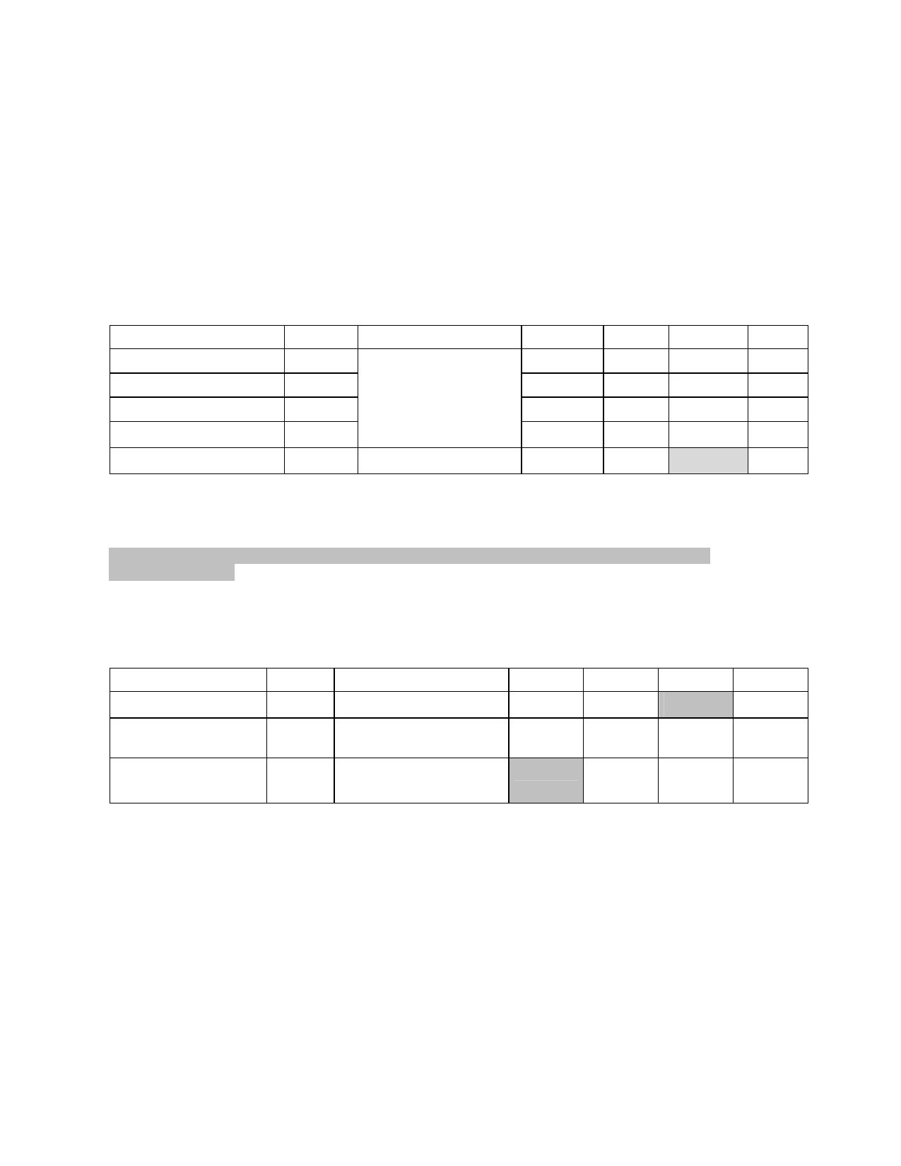
Table 20-15. Internal Flash ROM Electrical Characteristics (page 20-15)
(TA = –25 °C to + 85 °C, VDD = 2.0 V to 3.6 V)
Parameter
Symbol
Conditions
Programming Time (1)
Ftp
–
Chip Erasing Time (2)
Ftp1
Sector Erasing Time (3)
Ftp2
Data Access Time
FtRS
Number of Writing/Erasing FNWE
–
Min
Typ
Max
30
–
–
50
–
–
10
–
–
–
25
–
–
–
10,000(4)
NOTES:
1. The Programming time is the time during which one byte (8-bit) is programmed.
2. The Chip Erasing time is the time during which all 64K byte block is erased.
3. The Sector Erasing time is the time during which all 128 byte block is erased.
4. Maximum number of Writing/Erasing is 10,000 times for full-flash(S3F828B) and 100 times for half-flash
(S3F8289/F8285).
5. The Chip Erasing is available in Tool Program Mode only.
Unit
µs
ms
ms
ns
Times
Table 20-6. A/D Converter Electrical Characteristics
(TA = –25 °C to + 85 °C, VDD = 2.7 V to 3.6 V, VSS = 0 V)
Parameter
Symbol
Conditions
Analog input voltage
VIAN
–
Analog input
RAN
–
impedance
Analog reference
AVREF
–
voltage
Min
Typ
VSS
–
2
1000
2.0
–
Max
AVREF
–
VDD
Unit
V
MΩ
V
2. CHAPTHER 19. EMBEDDED FLASH MEMORY INTERFACE
This chapter is modified for only S3F828B.
3. CHAPTHER 12. 16-BIT TIMER 0/1
The Figure12-2 condition ‘Match signal’ should be moved in the page 12-3.
Share Link: 