S16008MK7TW-8A View Datasheet(PDF) - Unspecified
Part Name
Description
Manufacturer
S16008MK7TW-8A Datasheet PDF : 9 Pages
| |||
SYNCHRONOUS DRAM
Features:
• Intel PC-100 (3-3-3) or PC133 (3-3-3) compatible
• Fully synchronous; all signals registered on positive
edge of system clock
• Internal pipelined operation; column address can be
changed every clock cycle
• Internal banks for hiding row access precharge time
• Programmable burst lengths: 1, 2, or 4 using
Interleaved Burst Addressing
• Auto Precharge and Auto Refresh modes
• 64ms, 4,096-cycle refresh quad-row refresh,
(15.6µs/row)
• Self Refresh mode 1
• LVTTL-compatible inputs and outputs
• Single +3.3V ±0.3V power supply
• The x16 devices are optimized for both single and
dual rank DIMM applications. The x8 devices are
optimized for single rank DIMM applications.
Options:
Designation:
Family:
SpecTek Memory
SAA
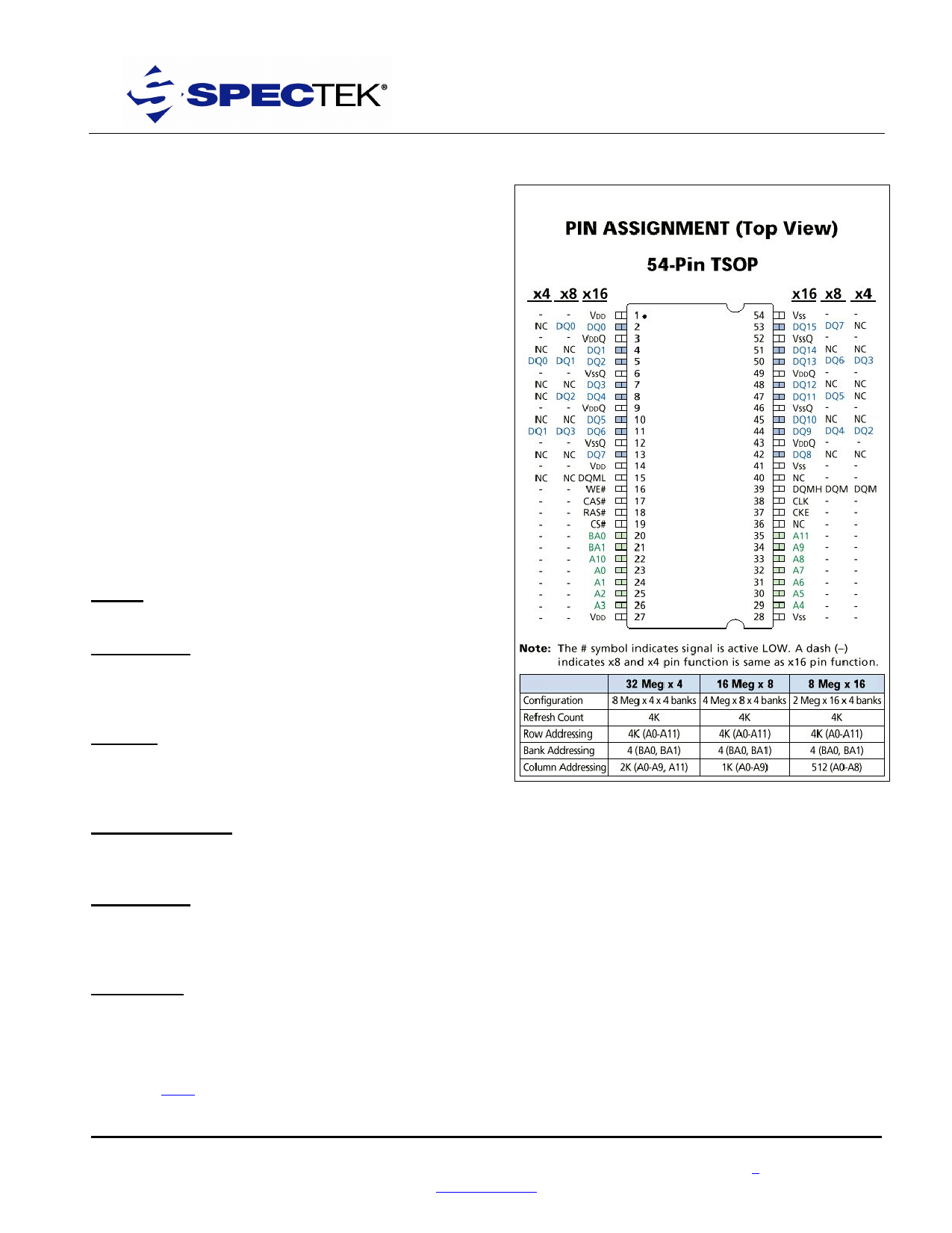
Configuration:
32 Meg x 4 (8 Meg x 4 x 4 banks)
16 Meg x 8 (4 Meg x 8 x 4 banks)
8 Meg x 16 (2 Meg x 16 x 4 banks)
32M4
16M8
8M16
Design ID
SDRAM 128 Megabit Design
(Call SpecTek Sales for details on
availability of “x” placeholders)
Yx5x
Voltage and Refresh:
3.3V, Auto Refresh, 4K refresh
L4
3.3V, Self or Auto Refresh1, 4K refresh M4
Package Types:
54-pin plastic TSOP (400 mil)
TK
60-ball FBGA (8mm x 16mm)
FB2
60-ball FBGA (11mm x 13mm)
FC2
Timing Types:
PC100 (3-3-3)
PC133 (3-3-3)
-8A
-75A
Part number example: SAA16M8Y95AL4TK-75A
(For part numbers prior to December
2004, refer to page 9 for decoding.)
128Mb: x4, x8, x16
SDRAM 3.3V
NOTES: 1. Only when specified. Consult Sales
2. Not available in x16 configuration
General Description:
The 128Mb SDRAM is a high-speed CMOS, dynamic
random-access memory containing 134,217,728 bits.
Each is internally configured as a quad-bank DRAM.
Read and write accesses to the SDRAM are burst
oriented; accesses start at a selected location and continue
for a programmed number of locations in a programmed
sequence. Accesses begin with the registration of an
ACTIVE command, which is then followed by a READ
or WRITE command. The address bits registered
coincident with the ACTIVE command are used to select
the bank and row to be accessed (BA0, BA1 select the
bank; A0-A11 select the row). The address bits registered
PDF: 09005aef807827f6 / Source: 09005aef807825bd
128Mb SDRAM
Rev: 11/29/2004
1
www.spectek.com
SpecTek reserves the right to change products or
specifications without notice. © 2001, 2002, 2004 SpecTek
Share Link: 