SC2453 View Datasheet(PDF) - Semtech Corporation
Part Name
Description
Manufacturer
SC2453 Datasheet PDF : 22 Pages
| |||
SC2453
POWER MANAGEMENT
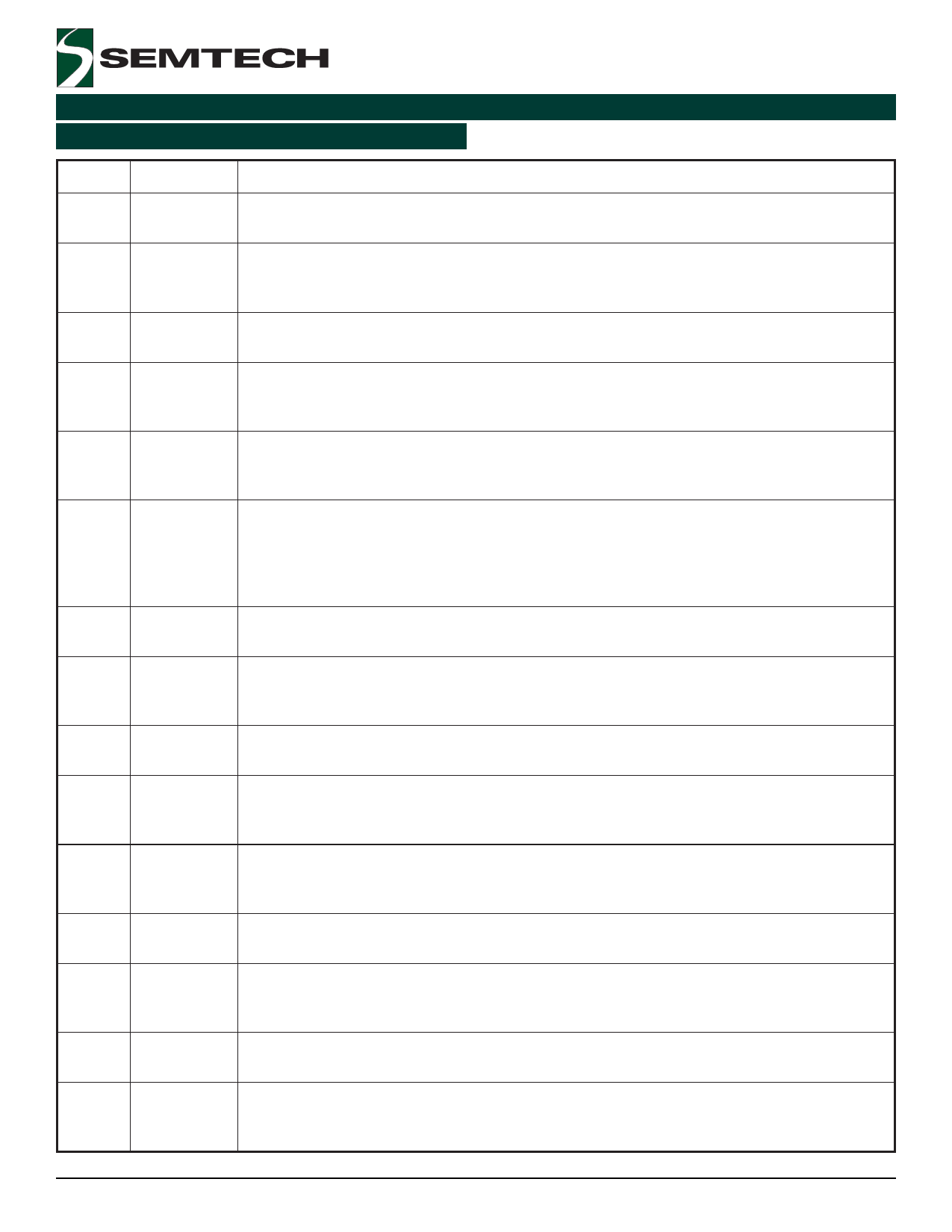
Pin Descriptions
Pin #
1
2
3
4
5
6
7
8
9
10
11
12
13
14
15
Pin Name
ILIM1
FB1
EO1
BD4
FB4
SS/SHDN
SYNC
POK
OSC
FB3
BD3
EO2
FB2
ILIM2
AGND
Pin Function
Adjustable current-limit pin set for the PWM switcher1. Connect a resistor from this pin to
AGND.
Voltage mode PWM switcher1 feedback input. Connect to a resistor-divider from output to
FB1 to AGND to adjust the output voltage between 0.5V and 0.9 x VIN as maximum duty cycle
allowed. The feedback set point is 0.5V.
The PWM switcher1 loop compensation pin. Connect a compensation network to compensate
the control loop. Type 3 compensation network is usually used.
Open-drain output PNP transistor driver. Internally connected to the drain of an N-channel
MOSFET. This pin connects to the base of an external PNP pass transistor to form a positive
linear regulator.
PNP transistor positive linear regulator feedback input. Connect to a resistor-divider between
the positive linear regulator and AGND to adjust the output voltage. The feedback set point is
0.5V.
The pin provides a soft-start function for the PWM switchers and positive linear regulator.
When the pin reaches 0.5V, the regulated 10uA pull-up current source charges the capacitor
connected from this pin to AGND. The error amplifier reference voltage of switcher1, switcher2
and positive linear regulators ramps from 0.7V to 2V respectively following the sequence. If the
pin is pulled down below 0.5V, the SC2453 is disabled.
The pin can be used to synchronize two or more controllers. This pin requires a 10K resistor to
AGND when it is not used.
Open-drain power-good output. POK is low when the output voltage is more than 10% below
or above the regulation point. POK is high impedance when the output is in regulation.
Connect a resistor between the pin and PVCC.
Oscillator frequency adjustable input. Connect a resistor between the pin and AGND to set the
PWM frequency.
NPN transistor negative linear regulator feedback input. Connect to a resistor-divider between
a positive reference voltage and the negative output to adjust the output voltage. The feedback
set point is 0V.
Open-drain output NPN transistor driver. Internally connected to the drain of a P-channel
MOSFET. This pin connects to the base of an external NPN pass transistor to form a negative
linear regulator.
The PWM switcher2 loop compensation pin. Connect a compensation network to compensate
the control loop. Type 3 compensation network is usually used.
Voltage mode PWM switcher2 feedback input. Connect to a resistor-divider from output to
FB2 to AGND to adjust the output voltage between 0.5V and 0.9 x VIN as maximum duty cycle
allowed. The feedback set point is 0.5V.
Adjustable current-limit pin set for the PWM switcher2. Connect a resistor from this pin to
AGND.
This is small signal ground and must be routed separately from the high current ground PGND.
All voltage levels are measured with respect to this pin. A ceramic capacitor should be
connected right to this pin for noise decoupling.
2005 Semtech Corp.
6
www.semtech.com
Share Link: 