SFH3219 View Datasheet(PDF) - OSRAM GmbH
Part Name
Description
Manufacturer
SFH3219 Datasheet PDF : 7 Pages
| |||
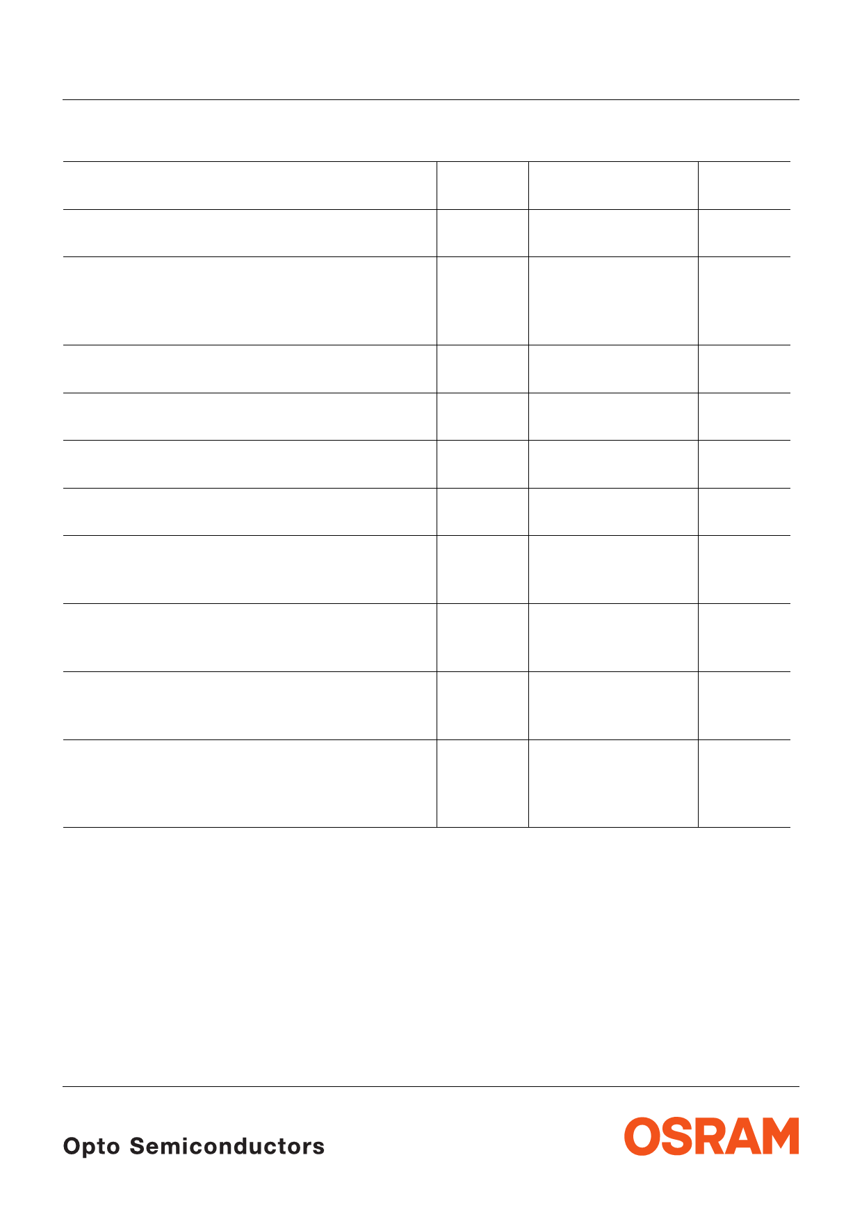
Kennwerte (TA = 25 °C, λ = 950 nm)
Characteristics
Bezeichnung
Parameter
Wellenlänge der max. Fotoempfindlichkeit
Wavelength of max. sensitivity
Spektraler Bereich der Fotoempfindlichkeit
S = 10% von Smax
Spectral range of sensitivity
S = 10% of Smax
Bestrahlungsempfindliche Fläche (∅ 240 µm)
Radiant sensitive area
Abmessung der Chipfläche
Dimensions of chip area
Halbwinkel
Half angle
Kapazität, VCE = 0 V, f = 1 MHz, E = 0
Capacitance
Dunkelstrom
Dark current
VCE = 20 V, E = 0
Fotostrom
Photo current
Ee = 0.1 mW/cm2, VCE = 5 V
Anstiegszeit/Abfallzeit
Rise and fall time
IC = 1 mA, VCC = 5 V, RL = 1 kΩ
Kollektor-Emitter-Sättigungsspannung
Collector-emitter saturation voltage
IC = 20 µA
Ee = 0.1 mW/cm2
Symbol
Symbol
λS max
λ
Wert
Value
990
430 … 1150
A
L×B
L×W
ϕ
CCE
ICEO
0.045
0.45 × 0.45
± 25
5.0
1 (≤ 50)
IPCE
≥ 63
tr, tf
7
VCEsat
150
SFH 3219
Einheit
Unit
nm
nm
mm2
mm × mm
Grad
deg.
pF
nA
µA
µs
mV
2001-11-22
3
Share Link: 