SMC032BF View Datasheet(PDF) - Numonyx -> Micron
Part Name
Description
Manufacturer
SMC032BF Datasheet PDF : 91 Pages
| |||
SMCxxxBF
Electrical interface
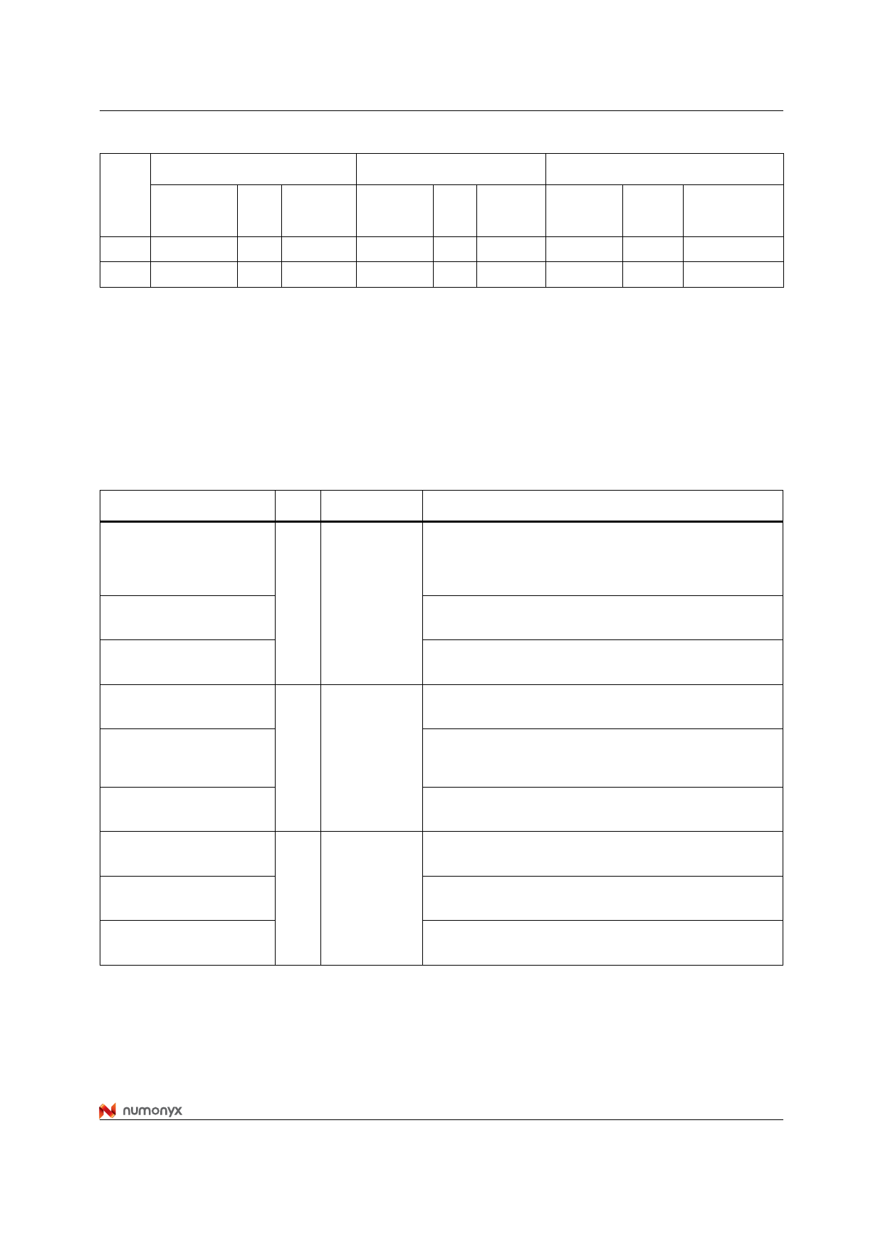
Table 8. Pin Assignment and Pin Type (continued)
Pin
Num
PC Card Memory Mode
Signal
Name
Pin In, Out
Type Type
PC Card I/O Mode
Signal
Name
Pin In, Out
Type Type
True IDE Mode
Signal
Name
Pin
Type
In, Out
Type
49
D10(3)
I/O I1Z,OZ3
D10(3)
I/O I1Z,OZ3 D10(3)
I/O
I1Z,OZ3
50
GND
Ground
GND
Ground
GND
Ground
1. For True IDE Mode, pin 9 is grounded.
2. The signal should be grounded by the host.
3. These signals are required only for 16 bit accesses and not required when installed in 8 bit systems. Devices should allow
for 3-state signals not to consume current.
4. The signal should be tied to VCC by the host.
5. The -CSEL signal is ignored by the Card in PC Card modes. However, because it is not pulled up on the Card in these
modes it should not be left floating by the host in PC Card modes. In these modes, the pin is normally connected by the
host to PC Card A25 or grounded by the host.
6. When the device does not operate in DMA mode, the signal should be held High or tied to VCC by the host. To ensure
proper operation with older hosts when DMA mode is disabled, the Card should ignore the –DMACK signal.
Table 9. Signal Description
Signal Name
Dir.
Pin
Description
A10 to A0
(PC Card Memory Mode)
A10 to A0
(PC Card I/O Mode)
A2 to A0
(True IDE Mode)
BVD1
(PC Card Memory Mode)
–STSCHG
(PC Card I/O Mode)
–PDIAG
(True IDE Mode)
BVD2
(PC Card Memory Mode)
–SPKR
(PC Card I/O Mode)
–DASP
(True IDE Mode)
8,10,11,12,
Used (with –REG) to select: the I/O port address registers,
the memory mapped port address registers, a Byte in the
Card information structure and its configuration control and
status registers.
I
14,15,16,17,
18,19,20 Same as PC Card Memory Mode
Only A2 to A0 are used to select the one of eight registers in
the Task File, the remaining lines should be grounded.
The battery voltage status of the Card, as no battery is
required it is asserted High.
Alerts the host to changes in the READY and Write Protect
I/O
46
states. Its use is controlled by the Card Configuration and
Status Register.
The Pass Diagnostic signal in the Master/Slave handshake
protocol.
The battery voltage status of the Card, as no battery is
required it is asserted High.
I/O
45
The Binary Audio output from the Card. It is asserted High
as audio functions are not supported.
This input/output is the Disk Active/Slave Present signal in
the Master/Slave handshake protocol.
17/91
Share Link: 