T89C51RD2-DDSI-L View Datasheet(PDF) - Atmel Corporation
Part Name
Description
Manufacturer
T89C51RD2-DDSI-L Datasheet PDF : 86 Pages
| |||
T89C51RD2
• The XRAM bytes can be accessed by indirect addressing, with EXTRAM bit cleared and MOVX instructions.
This part of memory which is physically located on-chip, logically occupies the first bytes of external data
memory. The bits XRS0 and XRS1 are used to hide a part of the available XRAM as explained in Table . This
can be useful if external peripherals are mapped at addresses already used by the internal XRAM.
• With EXTRAM = 0, the XRAM is indirectly addressed, using the MOVX instruction in combination with any
of the registers R0, R1 of the selected bank or DPTR. An access to XRAM will not affect ports P0, P2, P3.6
(WR) and P3.7 (RD). For example, with EXTRAM = 0, MOVX @R0, # data where R0 contains 0A0H,
accesses the XRAM at address 0A0H rather than external memory. An access to external data memory locations
higher than the accessible size of the XRAM will be performed with the MOVX DPTR instructions in the
same way as in the standard 80C51, so with P0 and P2 as data/address busses, and P3.6 and P3.7 as write and
read timing signals. Accesses to XRAM above 0FFH can only be done thanks to the use of DPTR.
• With EXTRAM = 1, MOVX @Ri and MOVX @DPTR will be similar to the standard 80C51. MOVX @ Ri
will provide an eight-bit address multiplexed with data on Port0 and any output port pins can be used to output
higher order address bits. This is to provide the external paging capability. MOVX @DPTR will generate a
sixteen-bit address. Port2 outputs the high-order eight address bits (the contents of DPH) while Port0 multiplexes
the low-order eight address bits (DPL) with data. MOVX @ Ri and MOVX @DPTR will generate either read
or write signals on P3.6 (WR) and P3.7 (RD).
The stack pointer (SP) may be located anywhere in the 256 bytes RAM (lower and upper RAM) internal data
memory. The stack may not be located in the XRAM.
The M0 bit allows to stretch the XRAM timings; if M0 is set, the read and write pulses are extended from 6 to
30 clock periods. This is useful to access external slow peripherals.
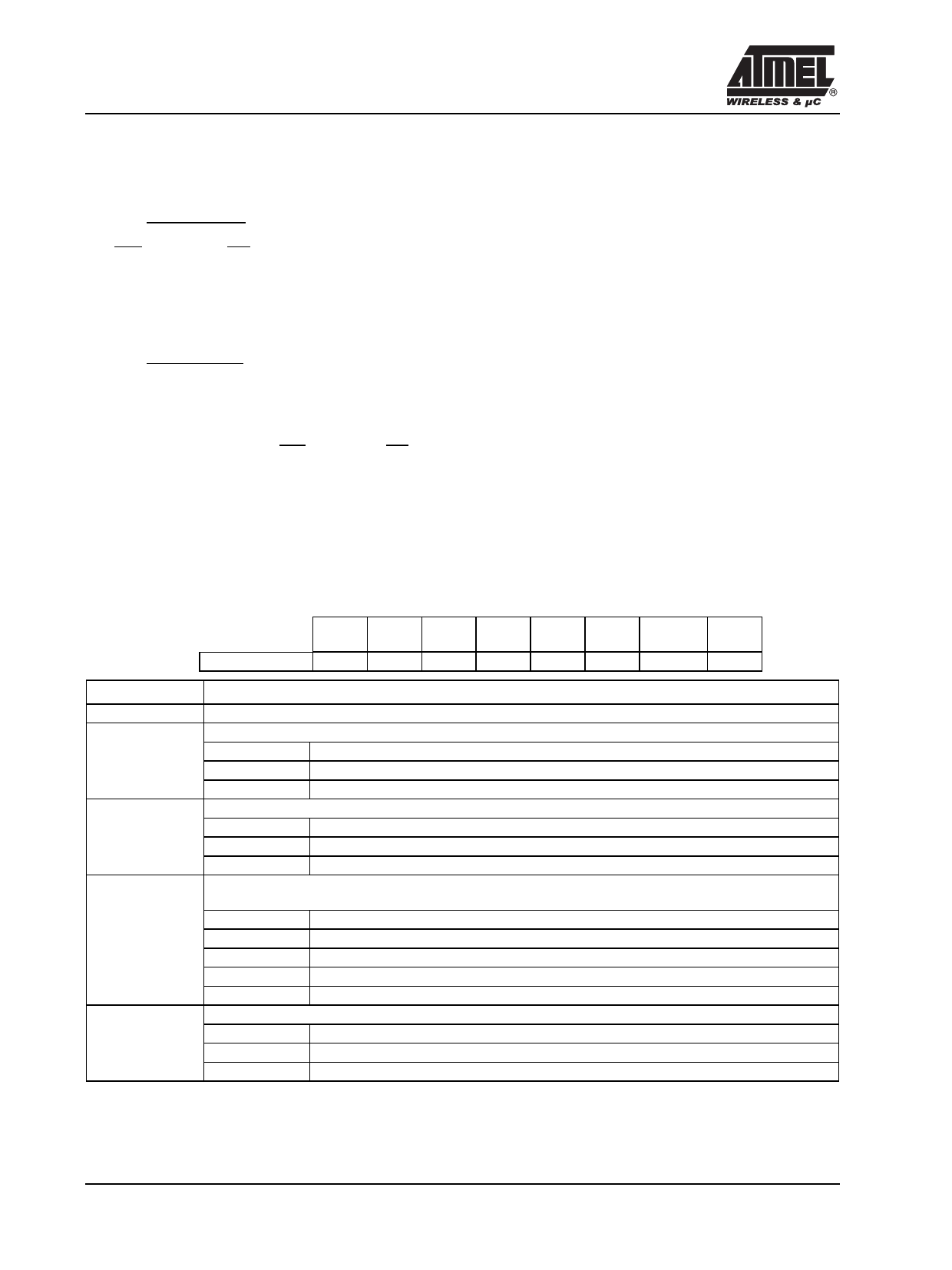
Auxiliary Register AUXR
AUXR
Address 08EH
Reset value
-
-
M0
-
XRS1 XRS0 EXTRAM AO
X
X
0
X
1
0
0
0
Symbol
-
AO
EXTRAM
XRS0
XRS1
M0
Function
Not implemented, reserved for future use.a
Disable/Enable ALE
AO
Operating Mode
0
ALE is emitted at a constant rate of 1/6 the oscillator frequency (or 1/3 if X2 mode is used)
1
ALE is active only during a MOVX or MOVC instruction
Internal/External RAM (00H-FFH) access using MOVX @ Ri/ @ DPTR
EXTRAM Operating Mode
0
Internal XRAM access using MOVX @ Ri/ @ DPTR
1
External data memory access
XRAM size: Accessible size of the XRAM
XRS1:0
XRAM size
00
256 bytes
01
512 bytes
10
768 bytes (default)
11
1024 bytes
Stretch MOVX control: the RD/ and the WR/ pulse length is increased according to the value of M0
M0
Pulse length in clock period
0
6
1
30
a. User software should not write 1s to reserved bits. These bits may be used in future 8051 family products to invoke new features. In
that case, the reset or inactive value of the new bit will be 0, and its active value will be 1. The value read from a reserved bit is
indeterminate.
16
Rev. F - 15 February, 2001
Share Link: 