SN54LS83AN View Datasheet(PDF) - Motorola => Freescale
Part Name
Description
Manufacturer
SN54LS83AN Datasheet PDF : 3 Pages
| |||
SN54 / 74LS83A
DC CHARACTERISTICS OVER OPERATING TEMPERATURE RANGE (unless otherwise specified)
Symbol
Parameter
Limits
Min Typ Max Unit
Test Conditions
VIH
Input HIGH Voltage
2.0
V
Guaranteed Input HIGH Voltage for
All Inputs
54
VIL
Input LOW Voltage
74
0.7
Guaranteed Input LOW Voltage for
0.8
V
All Inputs
VIK
VOH
Input Clamp Diode Voltage
54
Output HIGH Voltage
74
– 0.65 – 1.5
2.5
3.5
2.7
3.5
V
VCC = MIN, IIN = – 18 mA
V
VCC = MIN, IOH = MAX, VIN = VIH
V
per Truth Table
VOL
Output LOW Voltage
54, 74
74
0.25 0.4
0.35 0.5
V
IOL = 4.0 mA
VCC = VCC MIN,
VIN = VIL or VIH
V
IOL = 8.0 mA
per Truth Table
Input HIGH Current
C0
IIH
A or B
C0
A or B
20
µA VCC = MAX, VIN = 2.7 V
40
0.1
0.2
mA VCC = MAX, VIN = 7.0 V
Input LOW Current
IIL
C0
A or B
– 0.4 mA VCC = MAX, VIN = 0.4 V
– 0.8
IOS
Output Short Circuit Current (Note 1) – 20
–100 mA VCC = MAX
ICC
Power Supply Current
All Inputs Grounded
All Inputs at 4.5 V, Except B
All Inputs at 4.5 V
39
34
mA VCC = MAX
34
Note 1: Not more than one output should be shorted at a time, nor for more than 1 second.
AC CHARACTERISTICS (TA = 25°C)
Symbol
tPLH
tPHL
tPLH
tPHL
tPLH
tPHL
tPLH
tPHL
Parameter
Propagation Delay, C0 Input
to any Σ Output
Propagation Delay, Any A or
B Input to Σ Outputs
Propagation Delay, C0 Input
to C4 Output
Propagation Delay, Any A or
B Input to C4 Output
Limits
Min Typ Max Unit
16
24
ns
15
24
15
24
ns
15
24
11
17
ns
15
22
11
17
ns
12
17
Test Conditions
VCC = 5.0 V
CL = 15 pF
Figures 1 and 2
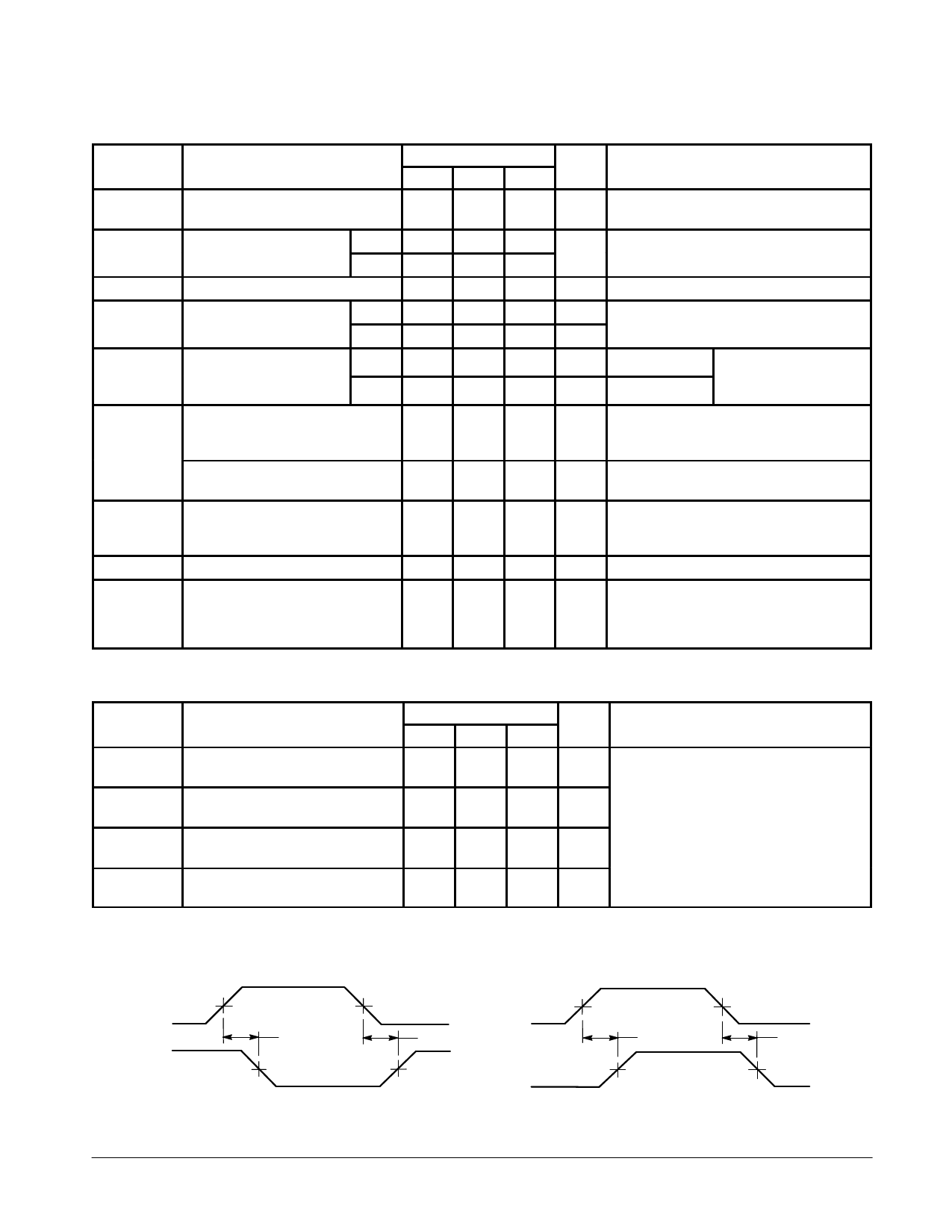
AC WAVEFORMS
VIN
VOUT
1.3 V
tPHL
1.3 V
1.3 V
tPLH
1.3 V
Figure 1
VIN
VOUT
1.3 V
tPLH
1.3 V
1.3 V
tPHL
1.3 V
Figure 2
FAST AND LS TTL DATA
5-83
Share Link: 