LC35W1000BM-10U View Datasheet(PDF) - SANYO -> Panasonic
Part Name
Description
Manufacturer
LC35W1000BM-10U Datasheet PDF : 9 Pages
| |||
LC35W1000BM, BTS-70U/10U
Notes: 1. The times tCOD1, tCOD2, tOOD, and tWOD are stipulated as the times until the output reaches the high-impedance
state. They are not stipulated by output voltage level.
2. Do not apply reverse phase signals to the data outputs when the data outputs are in the output state.
3. tWP is the period that CE1 and WE are at the low level and CE2 is at the high level, and is defined as the time
from the fall of WE until the rise of CE1 or WE or the fall of CE2, whichever occurs first.
4. tCW1 and tCW2 are the period that CE1 and WE are at the low level and CE2 is at the high level, and are defined
as the time from the fall of CE1 or the rise of CE2 to the rise of either CE1 or WE or the fall of CE2, whichever
occurs first.
5. The data outputs go to the high-impedance state when any one of the following states hold: OE is at the high
level, CE1 is at the high level, CE2 is at the low level, or WE is at the low level.
6. If OE is at the high level during the write cycle, the data outputs will go to the high-impedance state.
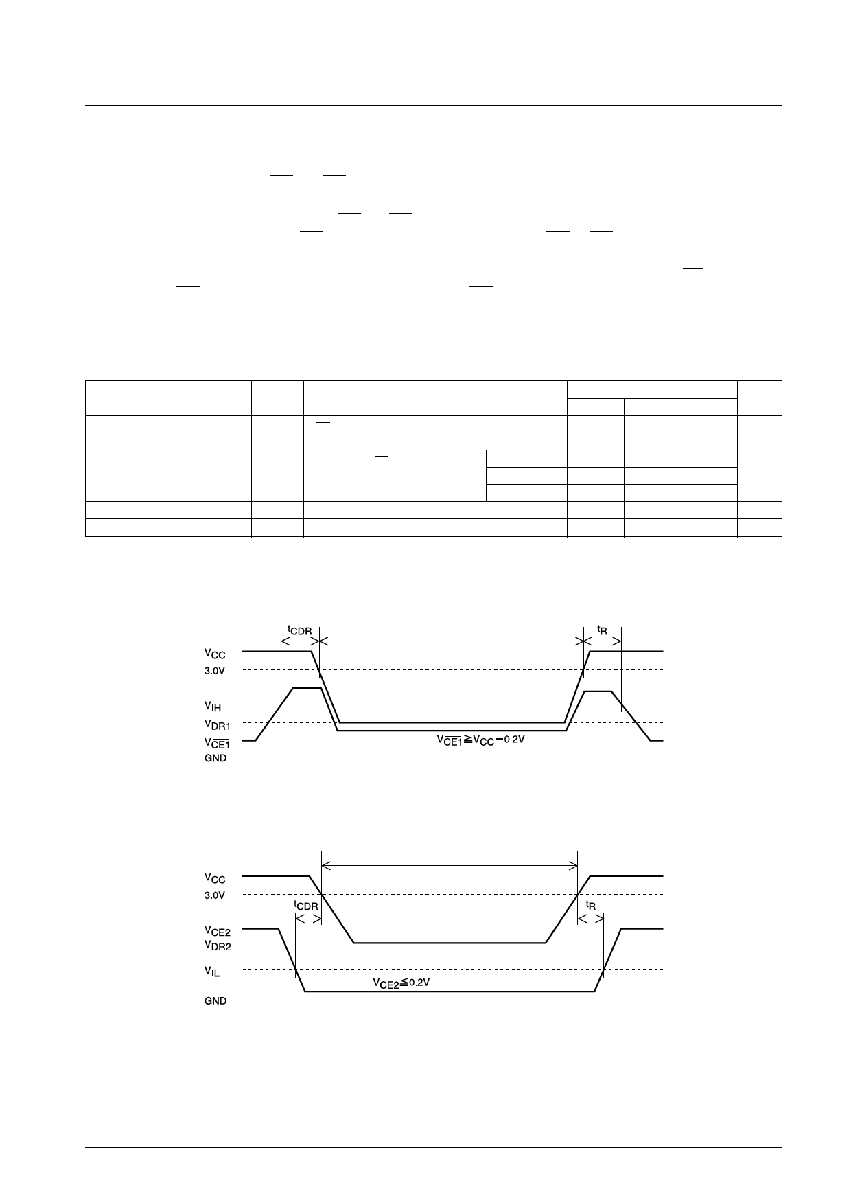
Data Retention Characteristics at Ta = –40 to +85°C
Parameter
Data retention supply voltage
Data retention supply current
Chip enable setup time
Chip enable hold time
Note: * Ta = +25°C
Symbol
Conditions
VDR1
VDR2
ICCDR1
tCDR
tR
VCE1 ≥ VCC – 0.2 V, VCE2 ≥ VCC – 0.2 V or VCE2 ≤ 0.2 V
VCE2 ≤ 0.2 V
VCC = 3.0 V, VCE1 ≥ VCC – 0.2 V,
–40°C to +85°C
VCE2 ≥ VCC – 0.2 V,
–40°C to +70°C
or VCE2 ≤ 0.2 V
+25°C
min
2.0
2.0
Ratings
typ
0.1
0
5
Unit
max
3.6
V
3.6
V
16
8
µA
ns
ms
Data Retention Waveforms (1) (CE1 control)
Data retention mode
Data Retention Waveforms (2) (CE2 control)
Data retention mode
A13494
A13495
No. 6624-8/9
Share Link: 