LC83010N View Datasheet(PDF) - SANYO -> Panasonic
Part Name
Description
Manufacturer
LC83010N Datasheet PDF : 18 Pages
| |||
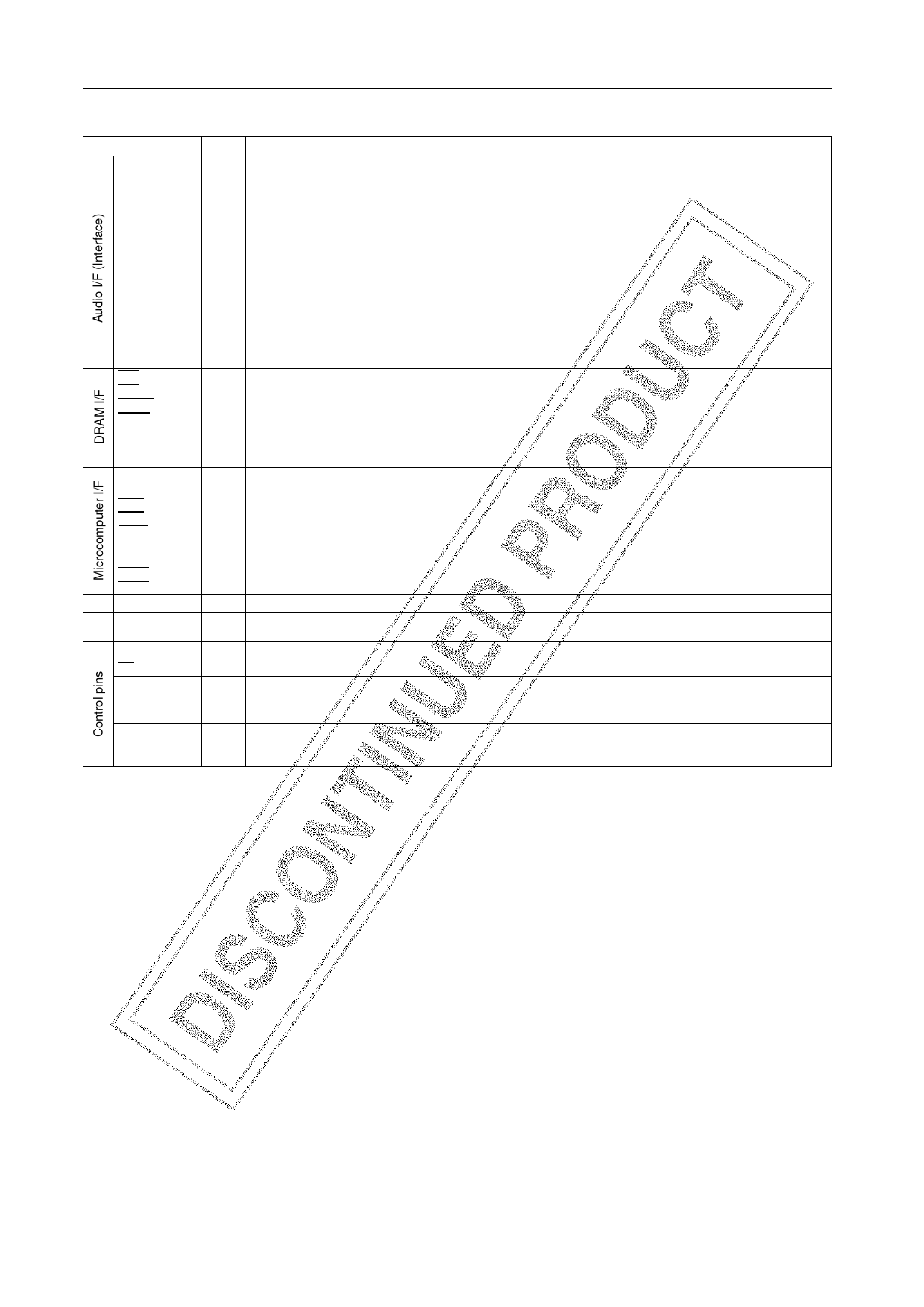
Pin Function
Pin Name
VDD1, 2
VSS1, 2
ASI1
ASI2
BCK1
BCK2
LRCKI
LRCKO
ASO
AOBCK
AOWCK
AOTDF1
AOTDF2
DFBCK
DFWCK
RAS
CAS
DREAD
DWRT
A0 to 8
D0 to 7
SI
SICK
SIRQ
SIAK
SRDY
SO
SOCK
SORQ
SOAK
P0 to 5
OSC1
OSC2
FS384O
INT
RES
SELC
TEST 1 to 4
FS64O/T5
LC83010N, 83010NE
I/O
Functional Description
I +5V power supply pins (These pins should be connected to the positive power source.)
I GND power supply pins (These pins should be connected to the ground level.)
I Audio data serial input 1
I Audio data serial input 2
I Bit clock input pin for ASI1 data
I/O Bit clock input pin for ASI2 data (I/O selectable by CR)
I Input pin for L/R channel distinguish signal (H: L channel data ; L: R channel data)
O Input pin for L/R channel distinguish signal (H: L channel data ; L: R channel data)
O Audio data serial output
O Bit clock output pin for ASO data (for 32fs and 48fs)
O Word clock output pin for ASO data
O Serial output pin for audio data (for high presence 1)
O Serial output pin for audio data (for high presence 2)
O Bit clock output pin for AOTDF1 and AOTDF2 data (for 32fs and 48fs)
O Word clock output pin for AOTDF1 and AOTDF2 data
O Output pin for RAS signal to external DRAMs
O Output pin for CAS signal to external DRAMs
O Output pin for data read signal to external DRAMs
O Output pin for data write signal to external DRAMs
O Output pins for address signals to external DRAMs (64K × 4 bits: A0 to A7, 256K × 4 bits: A0 to A8)
I/O Input/output pins for data transfer with external DRAMs. In the single DRAM configuration mode, pins D0 to D3 are
used. In the double DRAM configuration mode, pins D0 to D7 are used.
I Input pin for serial data from control microcomputer (8-bit serial data)
I Serial clock input pin for SI data
I Request signal input pin for serial data input
O Output pin for Acknowledge response to the input request signal from a microcomputer
I Input pin for a Ready signal from a controlling microcomputer indicating the end of a data transfer
O Output pin for serial data to a controlling microcomputer (8-bit serial data)
I Serial clock input pin for SO data
I Request signal input pin for serial data output
O Output pin for Acknowledge response to the output request signal from a microcomputer
I/O General-purpose Input/Output ports (with on-chip pull-up resistor)
I Pin for connection with a crystal oscillator or for clock input from an external source. (384fs)
O Pin for connection with a crystal oscillator ( should be left open in external clock input mode)
O 384fs output pin
I Interrupt request input pin (with on-chip pull-up resistor)
I Reset input pin (with on-chip pull-up resistor)
I
L/R channel signal select input pin with on-chip pull-down resistor ; L: external (LRCKI), H: internal (internal divider
output)
I Test signal input pins. Normally, these pins should be connected to the ground level.
O Test signal output pins. 64fs clock output/test output. FS64O/T5 funcitons as a test output in test mode and as a 64fs
clock output for external A/D converters during normal operation.
No.3945–4/18
Share Link: 