TC818ACBU View Datasheet(PDF) - Microchip Technology
Part Name
Description
Manufacturer
TC818ACBU Datasheet PDF : 24 Pages
| |||
TC818A
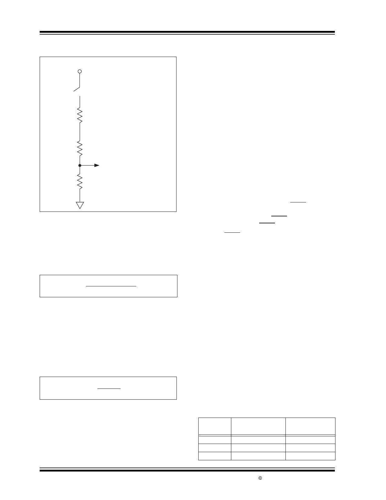
FIGURE 3-15:
RΩ CALCULATION (200Ω
MANUAL OPERATION)
VCC = 9V
SW33 RS ≈ 600Ω
R1
163.85Ω
R2
220Ω
VX
R3
300Ω
Analog Common = VCC – 3V
Where:
VANCOM = Potential at Analog Common ≈ 2.7V
RS
= 220Ω
RI
= 163.85Ω
RX
= 300Ω
RS
= Internal switch 33 resistance ≈ 600Ω
EQUATION 3-2:
RΩBUF =
(VCC – VANCOM)RX
(RX + RS + R1 + R8)
= 0.63V
For a 3.1V integrator swing, the value of RΩBUF is
easily calculated:
Where:
VINT
TI
CI
RXMAX
VXMAX
= Integrator swing = 3.1V
= Integration time = 100msec
= Integration capacitor = 0.1µF
= 300Ω
= 700mV
EQUATION 3-3:
RΩBUF = VXMAX(TI) = 200kΩ
CI(VINT)
With a low battery voltage of 6.6V, analog common will
be approximately 3.6V above the negative supply termi-
nal. With the integrator swinging down from analog com-
mon toward the negative supply, a 3.1V swing will set
the integrator output to 0.5V above the negative supply.
DS21475B-page 20
3.21 Capacitors - CINT, CAZ and CREF
The integration capacitor, CINT, must have low dielec-
tric absorption. A 0.1µF polypropylene capacitor is sug-
gested. The auto-zero capacitor, CAZ, and reference
capacitor, CREF, should be selected for low leakage
and dielectric absorption. Polystyrene capacitors are
good choices.
3.22 Reference Voltage Adjustment
The TC818A contains a low temperature drift internal
voltage reference. The analog common potential
(Pin 29) is established by this reference. Maximum drift
is a low 75ppm/°C. Analog common is designed to be
approximately 2.6V below VCC (Pin 28). A resistive
divider (R18/R19, Functional Diagram) sets the
TC818A reference input voltage (REFHI, Pin 34) to
approximately 163.85mV.
With an input voltage near full scale on the 200mV
range, R19 is adjusted for the proper reading.
3.23 Display Hold Feature
The LCD will not be updated when HOLD (Pin 60) is
connected to GND (Pin 58). Conversions are made, but
the display is not updated. A HOLD mode LCD annun-
ciator is activated when HOLD is low.
The LCD HOLD annunciator is activated through the
triplex LCD driver signal at Pin 13.
3.24 Flat Package Socket
Sockets suitable for prototype work are available. A
USA source is:
• Nepenthe Distribution
2471 East Bayshore, Suite 520
Palo Alto, CA 94303
(415) 856-9332
TWX: 910-373-2060
“CBQ” Socket, Part No. IC51-064-042
3.25 Resistive Ladder Networks
Resistor attenuator networks for voltage and resistance
measurements are available from:
• Caddock Electronics
1717 Chicago Avenue
Riverside, CA 92507
Tel: (714) 788-1700
TWX: 910-332-6108
TABLE 3-6: RESISTIVE LADDER
NETWORKS
Attenuator
Accuracy
0.1%
0.25%
0.25%
Attenuator Type
Voltage
Voltage
Resistance
Caddock
Part Number
1776-C441
1776-C44
T1794-204-1
© 2002 Microchip Technology Inc.
Share Link: 