SP504 View Datasheet(PDF) - Signal Processing Technologies
Part Name
Description
Manufacturer
SP504 Datasheet PDF : 31 Pages
| |||
FEATURES…
The SP504 is a highly integrated serial trans-
ceiver that allows software control of its inter-
face modes. Similar to the SP503, the SP504
offers the same hardware interface modes for
RS-232 (V.28), RS-422A (V.11), RS-449, RS-
485, V.35, EIA-530 and includes V.36 and
EIA-530A. The interface mode selection is done
via an 8–bit switch; four (4) bits control the
drivers and four (4) bits control the receivers.
The SP504 is fabricated using low power
BiCMOS process technology, and incorporates
a Sipex patented (5,306,954) charge pump
allowing +5V only operation. Each device is
packaged in an 80–pin JEDEC Quad FlatPack
package.
The SP504 is ideally suited for wide area net-
work connectivity based on the interface modes
offered and the driver and receiver configura-
tions. The SP504 has seven (7) independent
drivers and seven (7) independent receivers. In
V.35 mode, the SP504 includes the necessary
components and termination resistors internal
within the device for compliant V.35 operation.
THEORY OF OPERATION
The SP504 is made up of five separate circuit
blocks — the charge pump, drivers, receivers,
decoder and switching array. Each of these
circuit blocks is described in more detail below.
Charge–Pump
The SP504's charge pump design is based on the
SP503 where Sipex's patented charge pump
design (5,306,954) uses a four–phase voltage
shifting technique to attain symmetrical ±10V
power supplies. In addition, the SP504 charge
pump incorporates a "programmable" feature
that produces an output of ±10V or ±5V for VSS
and VDD depending on the mode of operation.
The charge pump still requires external capaci-
tors to store the charge. Figure 17a shows the
waveform found on the positive side of capaci-
tor C2, and Figure 17b shows the negative side
of capcitor C2. There is a free–running oscilla-
tor that controls the four phases of the voltage
shifting. A description of each phase follows.
The SP504 charge pump is used for RS-232
where the output voltage swing is typically
±10V and also used for RS-423. However, RS-
423 requires the voltage swing on the driver
output be between ±4V to ±6V during an open
circuit (no load). The charge pump would need
to be regulated down from ±10V to ±5V. A
typical ±10V charge pump would require exter-
nal clamping such as 5V zener diodes on VDD
and VSS to ground. The ±5V output has sym-
metrical levels as in the ±10V output. The ±5V
is used in the following modes where RS-423
levels are used: RS-449, EIA-530, EIA-530A
and V.36.
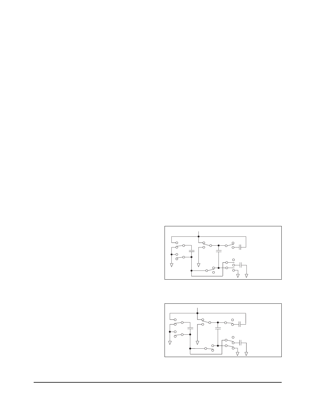
Phase 1 (±10V)
— VSS charge storage — During this phase of
the clock cycle, the positive side of capacitors
iiCss1tthraaennndssfCwe2rirtaecrdheetidonitCtoia2g–lr.loySucinnhdcaeargnCed2dt+htioesc+ch5oaVnrng. eeTcohtneedCCt1lo+–
+5V, the voltage potential across capacitor C2 is
now 10V.
Phase 1 (±5V)
— VSS & VDD charge storage and transfer —
cWtcgoharopia+turah5gcnVetidht,ooearCnn.CldS+C1iti1amhs–netuidhs5letCVtanr2nacsecnhwoasaupfiretsagcrlcerhyieettodohdnretstoCoCin2t2gh+–irteiioissauVsltnlwrSyadSinctascshtnfhoaederrrgdartehgetdodee
to the VDD storage capacitor.
VCC = +5V
+
C1 –
–5V
+5V
+
C2 –
–5V
C4
+ – VDD Storage Capacitor
– + VSS Storage Capacitor
C3
Figure 13a. Charge Pump Phase 1 for ±10V.
VCC = +5V
+
C1 –
–5V
+5V
+
C2 –
C4
+ – VDD Storage Capacitor
– + VSS Storage Capacitor
C3
Figure 13b. Charge Pump Phase 1 for ±5V.
Rev: A Date:1/27/04
SP504 Multi–Mode Serial Transceivers
13
© Copyright 2004 Sipex Corporation
Share Link: 