TSM108(2001) View Datasheet(PDF) - STMicroelectronics
Part Name
Description
Manufacturer
TSM108 Datasheet PDF : 13 Pages
| |||
TSM108
6.4. OVLO increase:
If the OVLO level needs to be increased (OV2), an
additional resistor (Rovl2) must be connected
between OV and Gnd following the equation.
u OV = Vref (Rovh/Rovl +1)
u OV2 = Vref (Rovh/(Rovl//Rovl2) +1) (iv)
where Rovl//Rovl2 means that Rovl2 is in parallel
to Rovl
Solving iv. we obtain:
u Rovl2 = Vref x Rovh Rovl / (OV2 x Rovl -
Vref x (Rovh + Rovl))
As an example, if OV2 needs to be set to 40V,
Rovl2 = 87kΩ
7. Standby Mode
In order to reduce to a minimum the current
consumption of the TSM108 when in inactive
phase, the Standby mode (!STBY pin of TSM108)
imposes a complete OFF state of the P-Channel
MOSFET, as well as a complete shut off of the
main functions of the TSM108 (operational
amplifier, PWM generator and oscillator, UVLO
and OVLO) and therefore reduces the
consumption of the TSM108 to the Istby value.
This !STBY command is TTL compatible, which
means that it can be directly commanded from
whatever logic signal.
8.Power Transistor: P-MOSFET or PNP
Transistor?
The TSM108 can drive, with minor external
components change, either a P-channel
MOSFET, or a PNP transistor. The choice of the
transistor is completely to the user’s responsibility,
nevertheless, here follows a few elements which
will help to decide which is the most adapted
transistor to drive depending on the application
characteristics in terms of power and
performances.
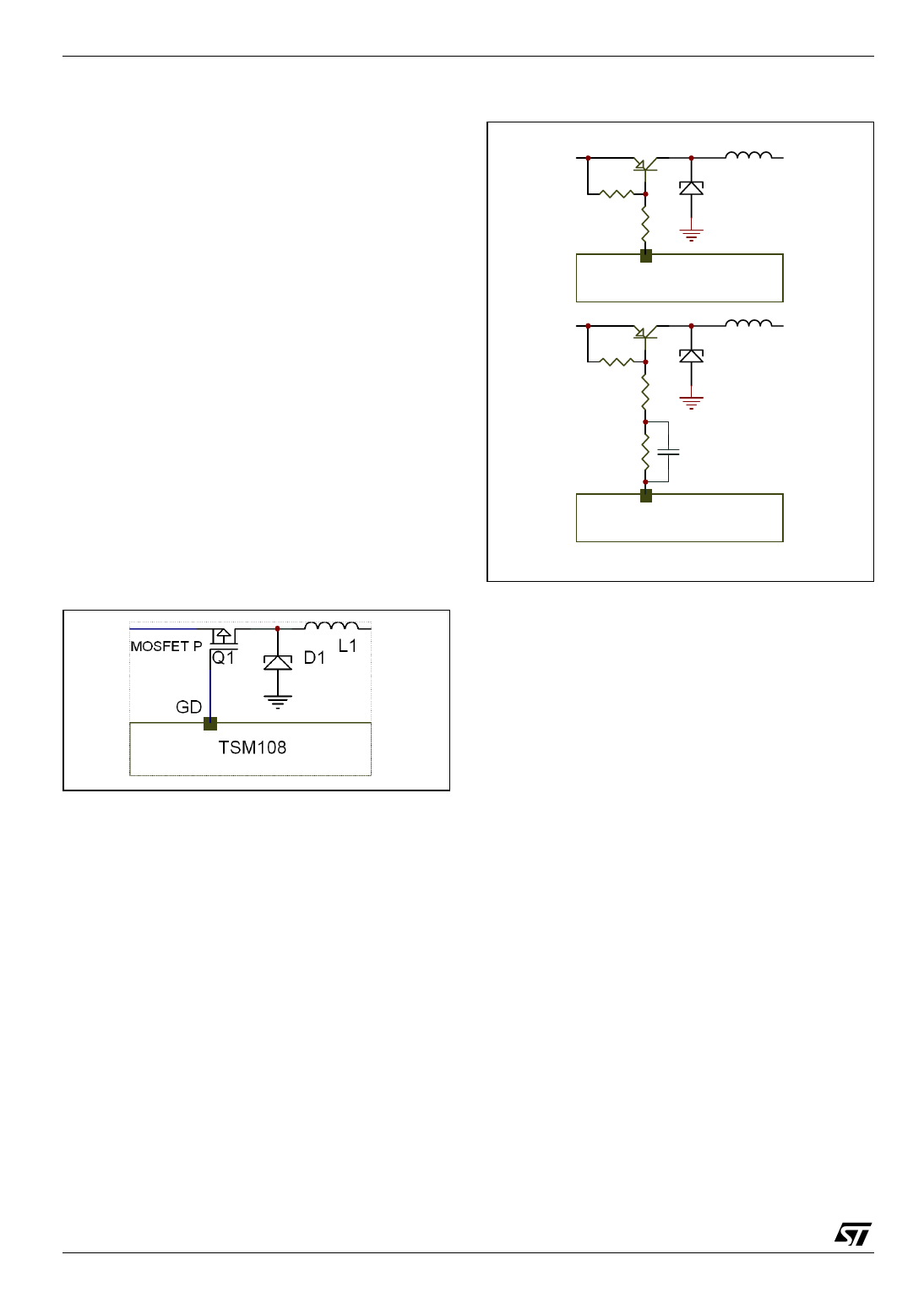
The following figures shows two different
schematics where both driving abilities of TSM108
are shown. The third schematic shows how to
improve the switch off commutation when using a
bipolar PNP transistor.
P- MOSFET? PNP Transistor?
MOSFET P
Q1
L1
D1
GD
TSM108
Q1
L1
D1
GD
TSM108
Q1
L1
D1
GD
TSM108
The most immediate way to choose from a
P-channel MOSFET or a PNP transistor is to
consider the ratio between the output power of the
application and the expected components price:
the lower the power, the more suitable the PNP
transistor is; the higher the power, the more
suitable the P-channel MOSFET is. As an
example, for a DC/DC adaptor built for 12V/6V,
the recommended limit to choose from one to the
other is situated around 200mA.
Below 200mA, the price/performance ratio of the
PNP transistor is very attractive, whereas above
200mA, the P-channel Mosfet takes the
advantage.
9. Calculation of the Passive Elements
Let’s consider the following characteristics for a
Cigarette Lighter Cellular Phone Battery Charger:
Vin = 12V - input voltage of the converter
Vout = 6V - output voltage of the converter
F = 100kHz - switching frequency of the converter
adjustable with an external capacitor
Iout = 625mA - output current limitation
9.1. Inductor
The minimum inductor value to choose should
apply to
Lmin = (1 - D) R / 2F
where R = Vout / Iout = 9.6Ω
and where D = Vout / Vin = 0.5
Therefore, Lmin = 24µH.
8/13
Share Link: 