SPCA751A-P101 View Datasheet(PDF) - Unspecified
Part Name
Description
Manufacturer
SPCA751A-P101
Unspecified

SPCA751A-P101 Datasheet PDF : 13 Pages
| |||
Preliminary
SPCA751A-P101
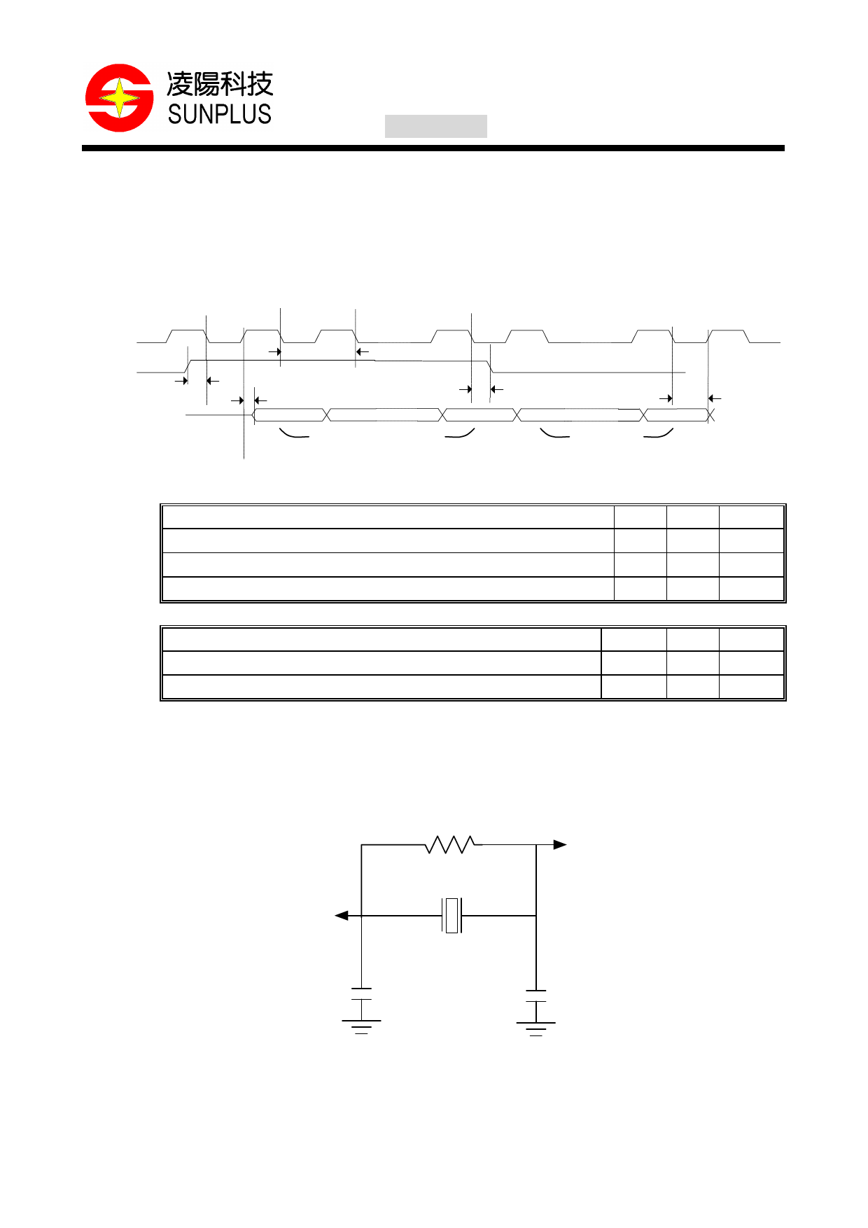
" Host processor reads 512 bytes from the SPCA751A
To read data from the SPCA751A, the host processor first asserts the TFS1 at the falling edges of SCLK1, then the
512-byte long data is sampled out from the SPCA751A at the following 512x8 consecutive rising edges of SCLK1. The
host processor is supposed to latch-in the data at the falling edges of SCLK1. TFS1 should remain high before the
MSB of the last word. After the LSB of the last word is received, the host processor should send at least three more
cycles of SCLK1 to the SPCA751A.
SCLK1
RFS1
DR1
TSCLK
TFS
TD
b15
b14
255 words
TFH
b0
b15
TDH
b0
Last word
Timing Requirements
PARAMETER
TFS
TFH
TSCLK
Switching Characteristics
PARAMETER
TD
TDH
TFS1 setup before SCLK1 falls low
TFS1 hold after SCLK1 falls low
SCLK1 period
DT1 access
DT1 hold after SCLK1 falls low
MIN.
2
2
16
MAX.
UNIT
ns
ns
ns
MIN.
MAX.
5
TSCLK / 2
UNIT
ns
ns
! PLL
An independent analog power is applied through pin 41 VSSP and pin 42 VDDP to supply the power for the
internal PLL. An oscillation circuit is built externally on pin 39 OSCIN and pin 40 OSCOUT.
10 M Ohm
pin 40
OSCOUT
pin 39
OSCIN
12 pF
16.934MHz
Crystal
12 pF
Oscillation Circuit
5
Share Link: