SST25VF010A View Datasheet(PDF) - Silicon Storage Technology
Part Name
Description
Manufacturer
SST25VF010A Datasheet PDF : 25 Pages
| |||
Data Sheet
Instructions
Instructions are used to Read, Write (Erase and Program),
and configure the SST25VF010A. The instruction bus
cycles are 8 bits each for commands (Op Code), data, and
addresses. Prior to executing any Byte-Program, Auto
Address Increment (AAI) programming, Sector-Erase,
Block-Erase, or Chip-Erase instructions, the Write-Enable
(WREN) instruction must be executed first. The complete
list of the instructions is provided in Table 6. All instructions
are synchronized off a high to low transition of CE#. Inputs
will be accepted on the rising edge of SCK starting with the
1 Mbit SPI Serial Flash
SST25VF010A
most significant bit. CE# must be driven low before an
instruction is entered and must be driven high after the last
bit of the instruction has been shifted in (except for Read,
Read-ID and Read-Status-Register instructions). Any low
to high transition on CE#, before receiving the last bit of an
instruction bus cycle, will terminate the instruction in
progress and return the device to the standby mode.
Instruction commands (Op Code), addresses, and data are
all input from the most significant bit (MSB) first.
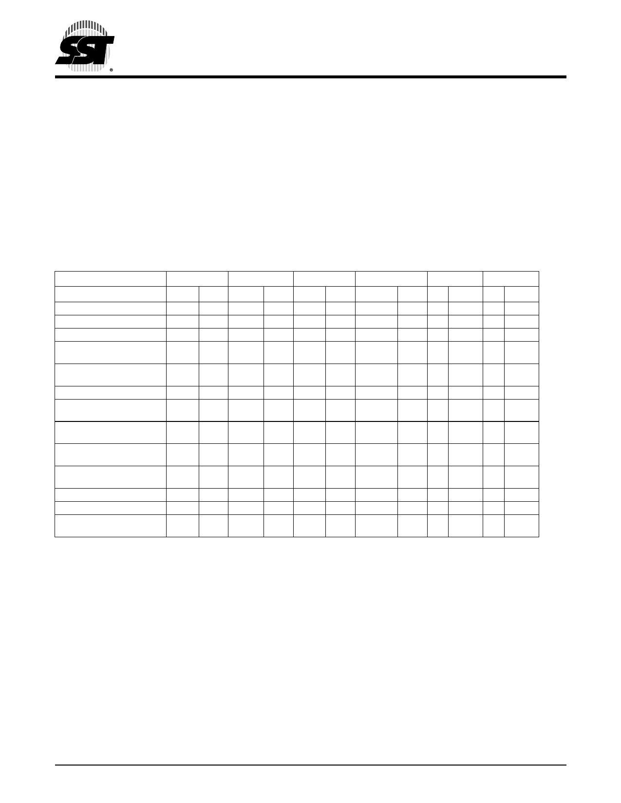
TABLE 6: DEVICE OPERATION INSTRUCTIONS1
Bus Cycle2
1
2
3
4
5
6
Cycle Type/Operation3,4
Read (20 MHz)
High-Speed-Read (33 MHz)
Sector-Erase5,6
Block-Erase5,7
Chip-Erase6
Byte-Program6
Auto Address Increment
(AAI) Program6,8
Read-Status-Register
(RDSR)
SIN
03H
0BH
20H
52H or
D8H
60H or
C7H
02H
AFH
05H
SOUT
Hi-Z
Hi-Z
Hi-Z
Hi-Z
Hi-Z
Hi-Z
Hi-Z
Hi-Z
SIN
A23-A16
A23-A16
A23-A16
A23-A16
-
A23-A16
A23-A16
X
SOUT
Hi-Z
Hi-Z
Hi-Z
Hi-Z
-
Hi-Z
Hi-Z
DOUT
SIN
A15-A8
A15-A8
A15-A8
A15-A8
-
A15-A8
A15-A8
-
SOUT
Hi-Z
Hi-Z
Hi-Z
Hi-Z
-
Hi-Z
Hi-Z
Note9
SIN
A7-A0
A7-A0
A7-A0
A7-A0
-
A7-A0
A7-A0
-
SOUT SIN SOUT SIN SOUT
Hi-Z X DOUT
Hi-Z X
X
X DOUT
Hi-Z -
-
Hi-Z -
-
-
-
-
Hi-Z DIN
Hi-Z DIN
Hi-Z
Hi-Z
Note9 - Note9
Hi-Z
Hi-Z
Note9
Enable-Write-Status-Register 50H Hi-Z
-
-
-
-
-
-
-
-
(EWSR)10
Write-Status-Register
(WRSR)10
01H Hi-Z Data Hi-Z
-
-
-.
-
-
-
Write-Enable (WREN)
06H Hi-Z
-
-
-
-
-
-
-
-
Write-Disable (WRDI)
Read-ID
04H Hi-Z
-
-
-
-
-
-
-
-
90H or Hi-Z 00H Hi-Z 00H Hi-Z ID Addr11 Hi-Z X DOUT12
ABH
DOUT12
1. AMS = Most Significant Address
T6.0 1265
AMS = A16 for SST25VF010A
Address bits above the most significant bit of each density can be VIL or VIH
2. One bus cycle is eight clock periods.
3. Operation: SIN = Serial In, SOUT = Serial Out
4. X = Dummy Input Cycles (VIL or VIH); - = Non-Applicable Cycles (Cycles are not necessary)
5. Sector addresses: use AMS-A12, remaining addresses can be VIL or VIH
6. Prior to any Byte-Program, AAI-Program, Sector-Erase, Block-Erase, or Chip-Erase operation, the Write-Enable (WREN)
instruction must be executed.
7. Block addresses for: use AMS-A15, remaining addresses can be VIL or VIH
8. To continue programming to the next sequential address location, enter the 8-bit command, AFH,
followed by the data to be programmed.
9. The Read-Status-Register is continuous with ongoing clock cycles until terminated by a low to high transition on CE#.
10. The Enable-Write-Status-Register (EWSR) instruction and the Write-Status-Register (WRSR) instruction must work in con-
junction of each other. The WRSR instruction must be executed immediately (very next bus cycle) after the EWSR instruction
to make both instructions effective.
11. Manufacturer’s ID is read with A0=0, and Device ID is read with A0=1. All other address bits are 00H. The Manufacturer’s and
Device ID output stream is continuous until terminated by a low to high transition on CE#
12. Device ID = 49H for SST25VF010A
©2006 Silicon Storage Technology, Inc.
8
S71265-02-000
1/06
Share Link: 