SST25VF020 View Datasheet(PDF) - Silicon Storage Technology
Part Name
Description
Manufacturer
SST25VF020 Datasheet PDF : 23 Pages
| |||
2 Mbit SPI Serial Flash
SST25VF020
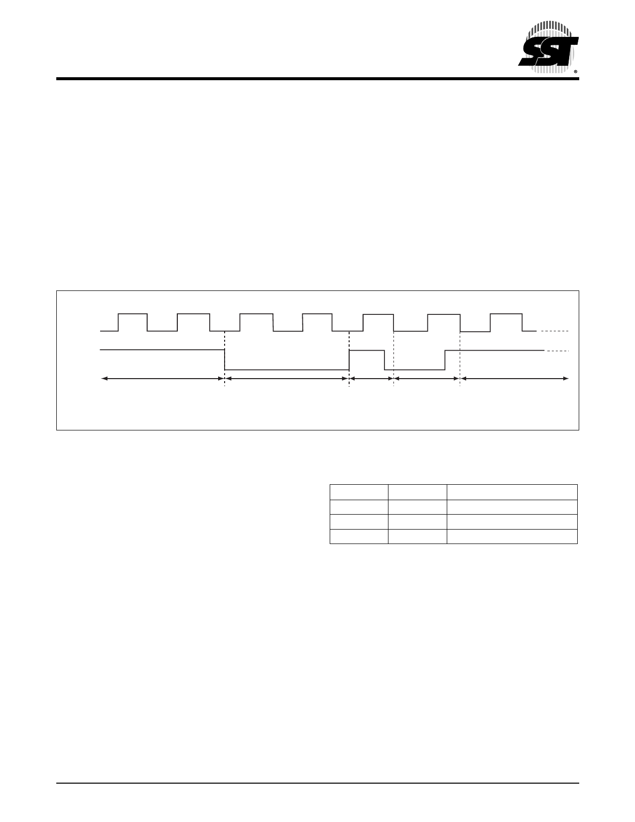
Hold Operation
HOLD# pin is used to pause a serial sequence underway
with the SPI flash memory without resetting the clocking
sequence. To activate the HOLD# mode, CE# must be in
active low state. The HOLD# mode begins when the SCK
active low state coincides with the falling edge of the
HOLD# signal. The HOLD mode ends when the HOLD#
signal’s rising edge coincides with the SCK active low state.
If the falling edge of the HOLD# signal does not coincide
with the SCK active low state, then the device enters Hold
mode when the SCK next reaches the active low state.
Similarly, if the rising edge of the HOLD# signal does not
Data Sheet
coincide with the SCK active low state, then the device
exits in Hold mode when the SCK next reaches the active
low state. See Figure 4 for Hold Condition waveform.
Once the device enters Hold mode, SO will be in high-
impedance state while SI and SCK can be VIL or VIH.
If CE# is driven active high during a Hold condition, it
returns the device to standby mode. As long as HOLD#
signal is low, the memory remains in the Hold condition. To
resume communication with the device, HOLD# must be
driven active high, and CE# must be driven active low. See
Figure 18 for Hold timing.
SCK
HOLD#
Active
Hold
Active
Hold
Active
1231 F03.0
FIGURE 4: Hold Condition Waveform
Write Protection
SST25VF020 provides software Write protection. The
Write Protect pin (WP#) enables or disables the lock-down
function of the status register. The Block-Protection bits
(BP1, BP0, and BPL) in the status register provide Write
protection to the memory array and the status register. See
Table 5 for Block-Protection description.
Write Protect Pin (WP#)
The Write Protect (WP#) pin enables the lock-down func-
tion of the BPL bit (bit 7) in the status register. When WP#
is driven low, the execution of the Write-Status-Register
(WRSR) instruction is determined by the value of the BPL
bit (see Table 3). When WP# is high, the lock-down func-
tion of the BPL bit is disabled.
TABLE 3: Conditions to execute Write-Status-
Register (WRSR) Instruction
WP#
L
L
H
BPL
1
0
X
Execute WRSR Instruction
Not Allowed
Allowed
Allowed
T3.0 1231
©2006 Silicon Storage Technology, Inc.
5
S71231-07-000
10/06
Share Link: 