SST25VF020 View Datasheet(PDF) - Silicon Storage Technology
Part Name
Description
Manufacturer
SST25VF020 Datasheet PDF : 23 Pages
| |||
2 Mbit SPI Serial Flash
SST25VF020
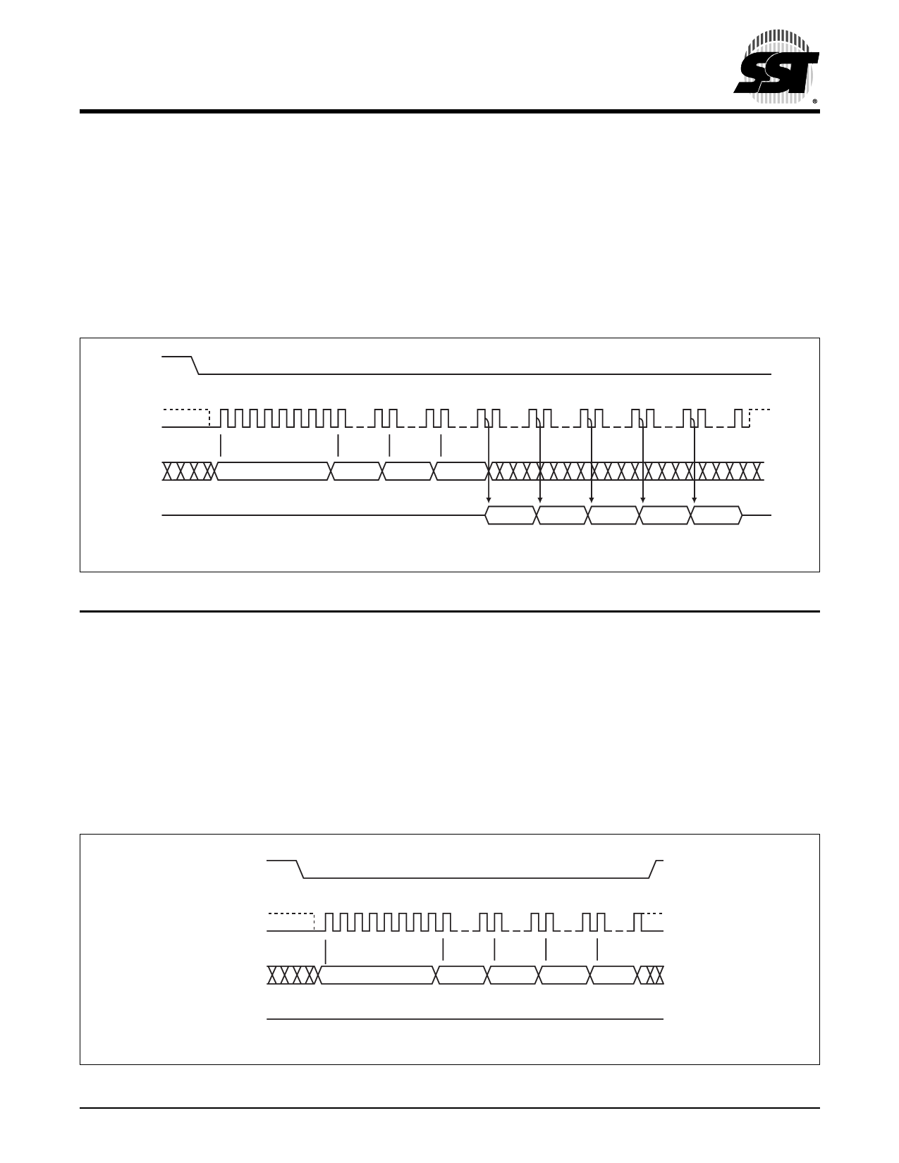
Read
The Read instruction outputs the data starting from the
specified address location. The data output stream is con-
tinuous through all addresses until terminated by a low to
high transition on CE#. The internal address pointer will
automatically increment until the highest memory address
is reached. Once the highest memory address is reached,
the address pointer will automatically increment to the
beginning (wrap-around) of the address space, i.e. for
Data Sheet
2 Mbit density, once the data from address location
3FFFFH had been read, the next output will be from
address location 00000H.
The Read instruction is initiated by executing an 8-bit com-
mand, 03H, followed by address bits [A23-A0]. CE# must
remain active low for the duration of the Read cycle. See
Figure 5 for the Read sequence.
CE#
MODE 3
SCK MODE 0
0 1 2345 6 78
15 16
23 24 31 32 39 40 47 48 55 56 63 64 70
SI
03
ADD. ADD. ADD.
MSB
MSB
HIGH IMPEDANCE
SO
N
DOUT
N+1
DOUT
N+2
DOUT
N+3
DOUT
N+4
DOUT
MSB
1231 F04.1
FIGURE 5: READ SEQUENCE
Byte-Program
The Byte-Program instruction programs the bits in the
selected byte to the desired data. The selected byte must
be in the erased state (FFH) when initiating a Program
operation. A Byte-Program instruction applied to a pro-
tected memory area will be ignored.
Prior to any Write operation, the Write-Enable (WREN)
instruction must be executed. CE# must remain active low
for the duration of the Byte-Program instruction. The Byte-
Program instruction is initiated by executing an 8-bit com-
mand, 02H, followed by address bits [A23-A0]. Following the
address, the data is input in order from MSB (bit 7) to LSB
(bit 0). CE# must be driven high before the instruction is
executed. The user may poll the Busy bit in the software
status register or wait TBP for the completion of the internal
self-timed Byte-Program operation. See Figure 6 for the
Byte-Program sequence.
CE#
MODE 3
SCK MODE 0
0 1 2345 6 78
15 16
23 24 31 32 39
SI
02
MSB
SO
FIGURE 6: Byte-Program Sequence
©2006 Silicon Storage Technology, Inc.
ADD.
MSB
ADD.
HIGH IMPEDANCE
ADD. DIN
MSB LSB
1231 F05.1
9
S71231-07-000
10/06
Share Link: 