MCP3201-BI/MS View Datasheet(PDF) - Microchip Technology
Part Name
Description
Manufacturer
MCP3201-BI/MS Datasheet PDF : 36 Pages
| |||

MCP3201
1.0 ELECTRICAL
CHARACTERISTICS
1.1 Maximum Ratings†
VDD...................................................................................7.0V
All inputs and outputs w.r.t. VSS ................ -0.6V to VDD +0.6V
Storage temperature .....................................-65°C to +150°C
Ambient temp. with power applied ................-65°C to +125°C
ESD protection on all pins (HBM) .................................> 4 kV
†Notice: Stresses above those listed under “Maximum
ratings” may cause permanent damage to the device. This is
a stress rating only and functional operation of the device at
those or any other conditions above those indicated in the
operational listings of this specification is not implied.
Exposure to maximum rating conditions for extended periods
may affect device reliability.
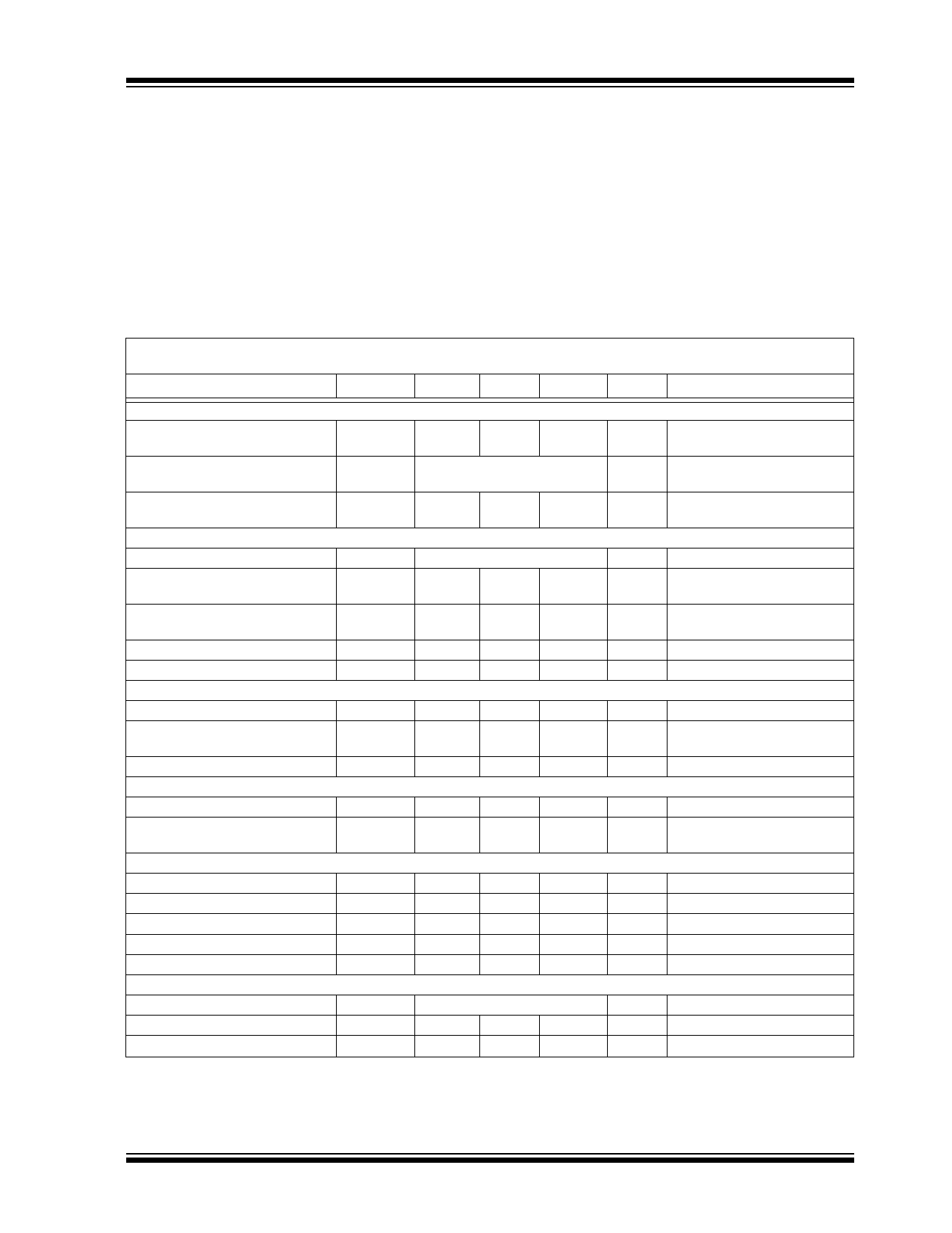
ELECTRICAL CHARACTERISTICS
Electrical Specifications: All parameters apply at VDD = 5V, VSS = 0V, VREF = 5V, TA = -40°C to +85°C, fSAMPLE = 100 ksps, and
fCLK = 16*fSAMPLE, unless otherwise noted.
Parameter
Sym
Min
Typ
Max
Units
Conditions
Conversion Rate:
Conversion Time
tCONV
—
—
12
clock
cycles
Analog Input Sample Time
tSAMPLE
1.5
clock
cycles
Throughput Rate
DC Accuracy:
fSAMPLE
—
—
100
ksps VDD = VREF = 5V
50
ksps VDD = VREF = 2.7V
Resolution
12
bits
Integral Nonlinearity
INL
—
±0.75
±1
LSB MCP3201-B
—
±1
±2
LSB MCP3201-C
Differential Nonlinearity
DNL
—
±0.5
±1
LSB No missing codes over
temperature
Offset Error
—
±1.25
±3
LSB
Gain Error
—
±1.25
±5
LSB
Dynamic Performance:
Total Harmonic Distortion
THD
—
-82
—
dB VIN = 0.1V to 4.9V@1 kHz
Signal to Noise and Distortion
(SINAD)
SINAD
—
72
—
dB VIN = 0.1V to 4.9V@1 kHz
Spurious Free Dynamic Range
SFDR
—
86
—
dB VIN = 0.1V to 4.9V@1 kHz
Reference Input:
Voltage Range
Current Drain
Analog Inputs:
0.25
—
VDD
—
100
150
—
.001
3
V Note 2
µA
µA CS = VDD = 5V
Input Voltage Range (IN+)
Input Voltage Range (IN-)
Leakage Current
IN+
IN-
—
VREF+IN-
V
IN-
VSS-100
VSS+100
mV
—
0.001
±1
µA
Switch Resistance
Sample Capacitor
Digital Input/Output:
RSS
—
1K
—
W See Figure 4-1
CSAMPLE
—
20
—
pF See Figure 4-1
Data Coding Format
Straight Binary
High Level Input Voltage
Low Level Input Voltage
VIH
0.7 VDD
—
—
V
VIL
—
—
0.3 VDD
V
Note 1:
2:
3:
This parameter is established by characterization and not 100% tested.
See graph that relates linearity performance to VREF level.
Because the sample cap will eventually lose charge, effective clock rates below 10 kHz can affect linearity performance,
especially at elevated temperatures. See Section 6.2 “Maintaining Minimum Clock Speed” for more information.
© 2008 Microchip Technology Inc.
DS21290E-page 3