SST25PF020B(2012) View Datasheet(PDF) - Microchip Technology
Part Name
Description
Manufacturer
SST25PF020B Datasheet PDF : 33 Pages
| |||
SST25PF020B
4.4 Software Status Register 1
The Software Status Register 1 is an additional register that
contains Top Sector and Bottom Sector Protection bits.
These register bits are read/writable and determine the lock
and unlock status of the top and bottom sectors. Table 4-3
describes the function of each bit in the Software Status
Register 1.
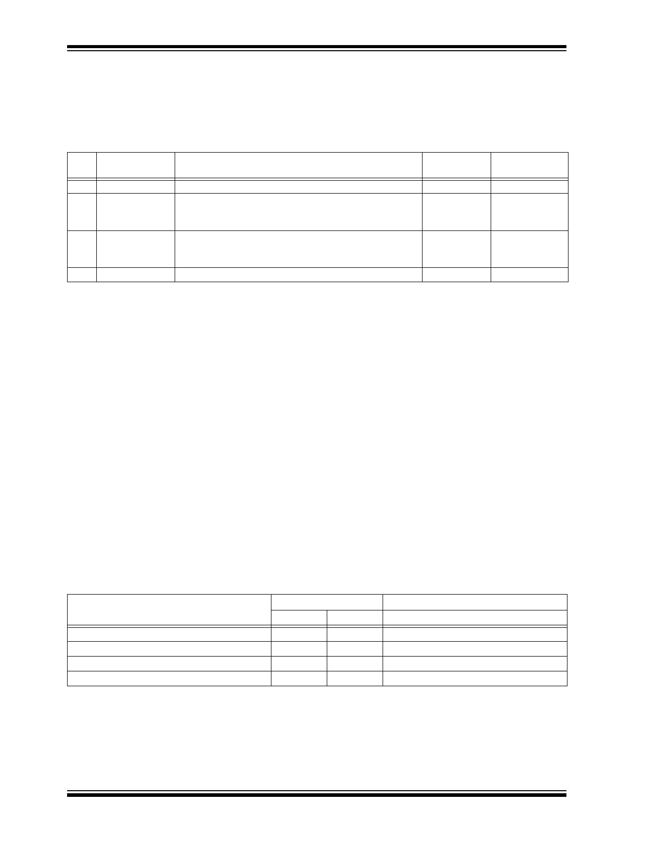
TABLE 4-3: SOFTWARE STATUS REGISTER 1
Bit Name
0:1 RES
2 TSP
3 BSP
4:7 RES
Function
Reserved for future use
Top Sector Protection status
1 = Indicates highest sector is write locked
0 = Indicates highest sector is Write accessible
Bottom Sector Protection status
1 = Indicates lowest sector is write locked
0 = Indicates lowest sector is Write accessible
Reserved for future use
Default at
Power-up
0
0
Read/Write
N/A
R/W
0
R/W
0
N/A
4.4.1 BUSY
The Busy bit determines whether there is an internal
Erase or Program operation in progress. A “1” for the
Busy bit indicates the device is busy with an operation
in progress. A “0” indicates the device is ready for the
next valid operation.
4.4.2 WRITE ENABLE LATCH (WEL)
The Write-Enable-Latch bit indicates the status of the
internal memory Write Enable Latch. If the Write-
Enable-Latch bit is set to “1”, it indicates the device is
Write enabled. If the bit is set to “0” (reset), it indicates
the device is not Write enabled and does not accept
any memory Write (Program/Erase) commands. The
Write-Enable-Latch bit is automatically reset under the
following conditions:
• Power-up
• Write-Disable (WRDI) instruction completion
• Byte-Program instruction completion
• Auto Address Increment (AAI) programming is
completed or reached its highest unprotected
memory address
• Sector-Erase instruction completion
• Block-Erase instruction completion
• Chip-Erase instruction completion
• Write-Status-Register instruction completion
4.4.3 AUTO ADDRESS INCREMENT (AAI)
The Auto Address Increment Programming-Status bit
provides status on whether the device is in AAI pro-
gramming mode or Byte-Program mode. The default at
power up is Byte-Program mode.
4.4.4 BLOCK PROTECTION (BP1, BP0)
The Block-Protection (BP1, BP0) bits define the size of
the memory area, as defined in Table 4-4, to be software
protected against any memory Write (Program or Erase)
operation. The Write-Status-Register (WRSR) instruc-
tion is used to program the BP1 and BP0 bits as long as
WP# is high or the Block-Protect-Lock (BPL) bit is 0.
Chip-Erase can only be executed if Block-Protection bits
are all 0. After power-up, BP1 and BP0 are set to 1.
TABLE 4-4:
SOFTWARE STATUS REGISTER BLOCK PROTECTION FOR SST25PF020B1
Status Register Bit2
Protected Memory Address
Protection Level
BP1
BP0
2 Mbit
0
0
0
None
1 (1/4 Memory Array)
0
1
030000H-03FFFFH
1 (1/2 Memory Array)
1
0
020000H-03FFFFH
1 (Full Memory Array)
1
1
000000H-03FFFFH
1. X = Don’t Care (RESERVED) default is ‘0’
2. Default at power-up for BP1 and BP0 is ‘11’. (All Blocks Protected)
DS25135A-page 6
2012 Microchip Technology Inc.
Share Link: 