F272-BAR-P View Datasheet(PDF) - STMicroelectronics
Part Name
Description
Manufacturer
F272-BAR-P Datasheet PDF : 188 Pages
| |||
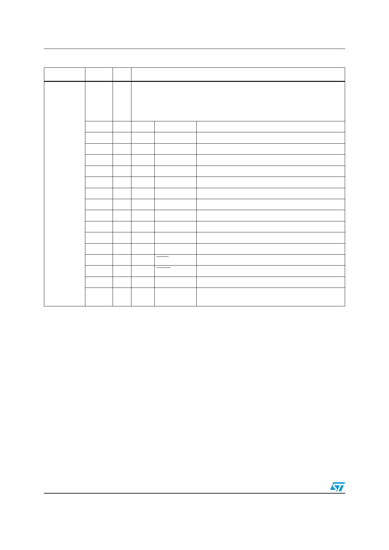
Pin data
ST10F272B/ST10F272E
Table 1. Pin description (continued)
Symbol
Pin Type
Function
65-70,
73-80,
81
15-bit (P3.14 is missing) bidirectional I/O port, bit-wise programmable for input or
I/O output via direction bit. Programming an I/O pin as input forces the corresponding
I/O output driver to high impedance state. Port 3 outputs can be configured as push-
I/O pull or open drain drivers. The input threshold of Port 3 is selectable (TTL or
CMOS). The following Port 3 pins have alternate functions:
65
I P3.0 T0IN
CAPCOM1: timer T0 count input
66
O P3.1 T6OUT
67
I P3.2 CAPIN
GPT2: timer T6 toggle latch output
GPT2: register CAPREL capture input
68
O P3.3 T3OUT
GPT1: timer T3 toggle latch output
69
I P3.4 T3EUD
GPT1: timer T3 external up/down control input
70
P3.0 - P3.5
P3.6 - P3.13, 73
P3.15
74
I P3.5 T4IN
I P3.6 T3IN
I P3.7 T2IN
GPT1; timer T4 input for count/gate/reload/capture
GPT1: timer T3 count/gate input
GPT1: timer T2 input for count/gate/reload / capture
75
I/O P3.8 MRST0
SSC0: master-receiver/slave-transmitter I/O
76
I/O P3.9 MTSR0
SSC0: master-transmitter/slave-receiver O/I
77
O P3.10 TxD0
78
I/O P3.11 RxD0
ASC0: clock / data output (asynchronous/synchronous)
ASC0: data input (asynchronous) or I/O (synchronous)
79
O P3.12 BHE
External memory high byte enable signal
WRH
External memory high byte write strobe
80
I/O P3.13 SCLK0
81
O P3.15 CLKOUT
SSC0: master clock output / slave clock input
System clock output (programmable divider on CPU
clock)
18/188
Doc ID 11917 Rev 3
Share Link: 