STV0042 View Datasheet(PDF) - STMicroelectronics
Part Name
Description
Manufacturer
STV0042 Datasheet PDF : 37 Pages
| |||
STV0042/STV0056 APPLICATION NOTE
3 - APPLICATION NOTES (continued)
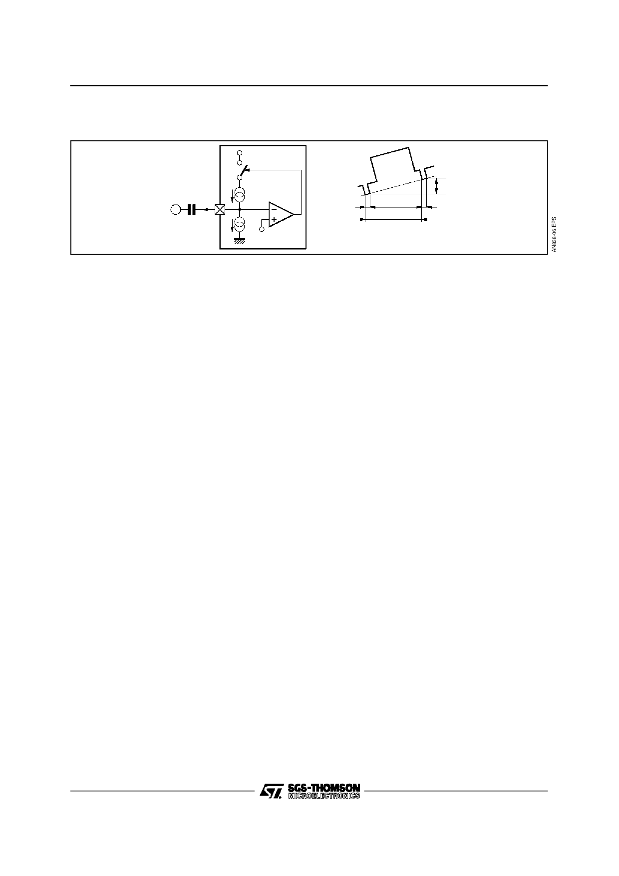
Figure 6 : Video Input Clamp Function
Filtered
Unclamped
Video
I2
A
C11
I1
2.7V
Video
∆
Ts
T
I CH = I2 - I 1 during Ts
I CH = - I1 during T - Ts
3.1.2.2 - Switching Matrix
This switching matrix is simply an array of CMOS
switches which is driven by registers. All configura-
tions are possible. Any output can be connected to
any input. An input can be connected to several
outputs.
3.1.2.3 - Output Stages
Each video output has a 6dB output gain, and the
internal final stage is a emitter follower structure
pulled down with a 1.3mA current source.
The output voltage amplitude is 2VPP, and the
synchro bottom level is clamped at 1.3V typically.
In the application, an external current amplifier
(75Ω driver) is required.
Remarks :
- The S3VIDOUT of the STV0056 features a black
level adjust (corresponding to a DC level adjust).
This function may be used to more simply inter-
face with built-in Videocrypt decoder.
- When the high 2 low power mode is selected, the
output impedance becomes high (≈ 23kΩ typ.),
and the DC output levels drops to low values
(< 0.2V) consequently the external 75Ω driver is
also turned (power saving).
3.2 - FM Demodulation
3.2.1 - Hardware Description
This chapter is relevant to :
- the input filter,
- a study of the FM demodulatorwhich is integrated
in the STV42/56 circuits (including the external
components needed at Pins DET L/R, AM-
PLOCK L/R, CPUMP L/R, AGC L/R).
3.2.1.1 - Input Filter (C25, R18, R17, L4, C24, C23)
The FM demodulator integrated in the STV42/56
circuit havea goodrejection of the video signal (due
to the selective AGC stage see paragraph 3.2.1.2).
However, to get a good audio signal to noise ratio,
it is preferable to attenuate the video signal spec-
trum with an input filter.
The filter proposed in the typical application (see
Figure 7) contains a high pass cell (C25, R18,
fC ≈ 1.5MHz) and a chroma trap (R17, L4, C24).
C23 is required for capacitive coupling with the
FM IN Pin (C23 value is not critical).
The center frequency of the chroma trap is about
4.4MHz for PAL/SECAM application and 3.58MHz
in case of NTSC application (Remark : In case of
PAL/NTSC application, a double trap may be re-
quired.)
It is recommanded to directly connect the input filter
to the tuner baseband output,because at this stage
the video signal is still emphazed (giving a natural
14dB attenuation of the lower part of the video
spectrum where most of the energy is concen-
trated.
3.2.1.2 - FM Demodulators
The block diagram of the FM demodulation part is
given in Figure 8. This block diagram contains 2
independants FM demodulators able to process all
types of mono and stereo sound, including :
- mono signals with deviation from ± 30kHz up to
± 400kHz (remark the spec mentions : ± 19.5kHz
to ± 592kHz, in order to cover all possible disper-
sions).
- Stereo pair featuring a frequency spacing differ-
ent from 180kHz (between left and right sub-car-
riers).
Each FM demodulator section contains 2 parts :
- an automatically gain controlled input stage
- a PLL demodulator
The only common point to both FM demodulators
is the frequency synthesis circuit : SYNTHE-
SIZER.
The structure of the FM demodulators which is
different from conventional solutions have been
selected for the two following reasons :
- no need for costly selective filters(LC or ceramic),
- to have a variable bandwidth (to accomodate all
type of deviations).
7/37
Share Link: 