TB2110FN View Datasheet(PDF) - Toshiba
Part Name
Description
Manufacturer
TB2110FN Datasheet PDF : 19 Pages
| |||
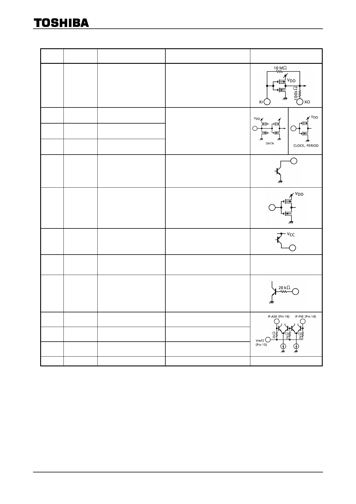
Pin Function
Pin No.
Symbol
Pin Name
Function
1
XI
2
XO
Crystal oscillator pins
3
Data
4
Clock
5
Period
6
Out-1
7
Out-2
8
Out-3
9
Out-4
Serial data input /
output
Clock signal input
Period signal input
General-purpose
output port
Connect a 75kHz crystal
oscillator for the reference
frequency to these pins.
Serial I / O port.
Use this pin to set the
divide ratio and divide
method, as well as transfer
data to and from the
controller to control the
general-purpose counter and
general-purpose I / O port.
This is an open-collector
output port.
Use this port to output
control signals.
10 In port
General-purpose input
port
This port accepts the data
to be fed to the output bit
(out-5).
11
VCONT
12 VDD
DC / DC converter
control pin
CMOS section power
supply
13 Stand-by
Standby
14 IF-FM
15
VREF2
16 IF-AM
17 A-GND
General-purpose
counter input
Reference pin
General-purpose
counter input
Bipolar section GND
This pin controls the DC / DC
converter.
The VDD power supply from
the DC / DC converter is
applied to this pin.
The device is placed in
standby mode when a “L” is
input.
The device is in active state
when a “H” is input.
Use this pin for IF signal
input on the FM side.
Use this pin as the reference
of the IF signal.
Use this pin for IF signal
input on the AM side.
—
TB2110FN
Remarks
—
—
4
2002-10-30
Share Link: 