TB2110FN View Datasheet(PDF) - Toshiba
Part Name
Description
Manufacturer
TB2110FN Datasheet PDF : 19 Pages
| |||
TB2110FN
Operation
○ Serial I / O port
The TB2110FN has two pairs of 24 bit registers, so it can set data to a total of 48 bits to control each function.
Each data in these registers are transferred to and from the controller through a serial port using three pins:
Data, clock, and period. A total of 32 bits consisting of 8 bit address and 24 data bits can be handled in one serial
transfer.
Because all operations are controlled via register, this section describes mainly the function of 8 bit address and
each register. The registers are configured in units of 24 bits, and are selected by an 8 bit address. The address
mapping of each register is listed in the next page as “register allocation.”
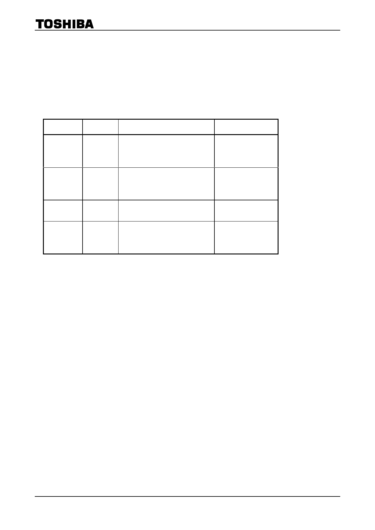
Register
Input
register 1
Input
register 2
Output
register 1
Output
register 2
Address
D0H
Contents Of 24 Bits
PLL dividend number setting
Reference frequency setting
PLL input and mode setting
Not used
D2H
General-purpose counter control
Test bit
Output data
Not used
D1H
General-purpose counter numeric data
Not used
D3H
Data in register D2
Lock detection data
Input data
Not used
No. Of Bits
16
3
2
3
Total 24
7
1
4
12
Total 24
22
2
Total 24
8
2
1
13
Total 24
The input data is latched into register 1 or register 2 at the falling edge of period to put each function to work.
The output data that comes in parallel is latched into the output register at the 9 th falling edge of clock, and is
serially output from the data pin.
(Note) Transmit dummy data at least once before transferring regular data to initialize the device’s internal circuits
after power-on.
6
2002-10-30
Share Link: 