TB2922HQ View Datasheet(PDF) - Toshiba
Part Name
Description
Manufacturer
TB2922HQ Datasheet PDF : 15 Pages
| |||
TB2922HQ
Caution and Application Method (Description is made only on the single channel)
1. Voltage Gain Adjustment
This IC has no NF (negative feedback) Pins. Therefore, the voltage gain can not be adjusted, but it makes
the device a space and total costs saver.
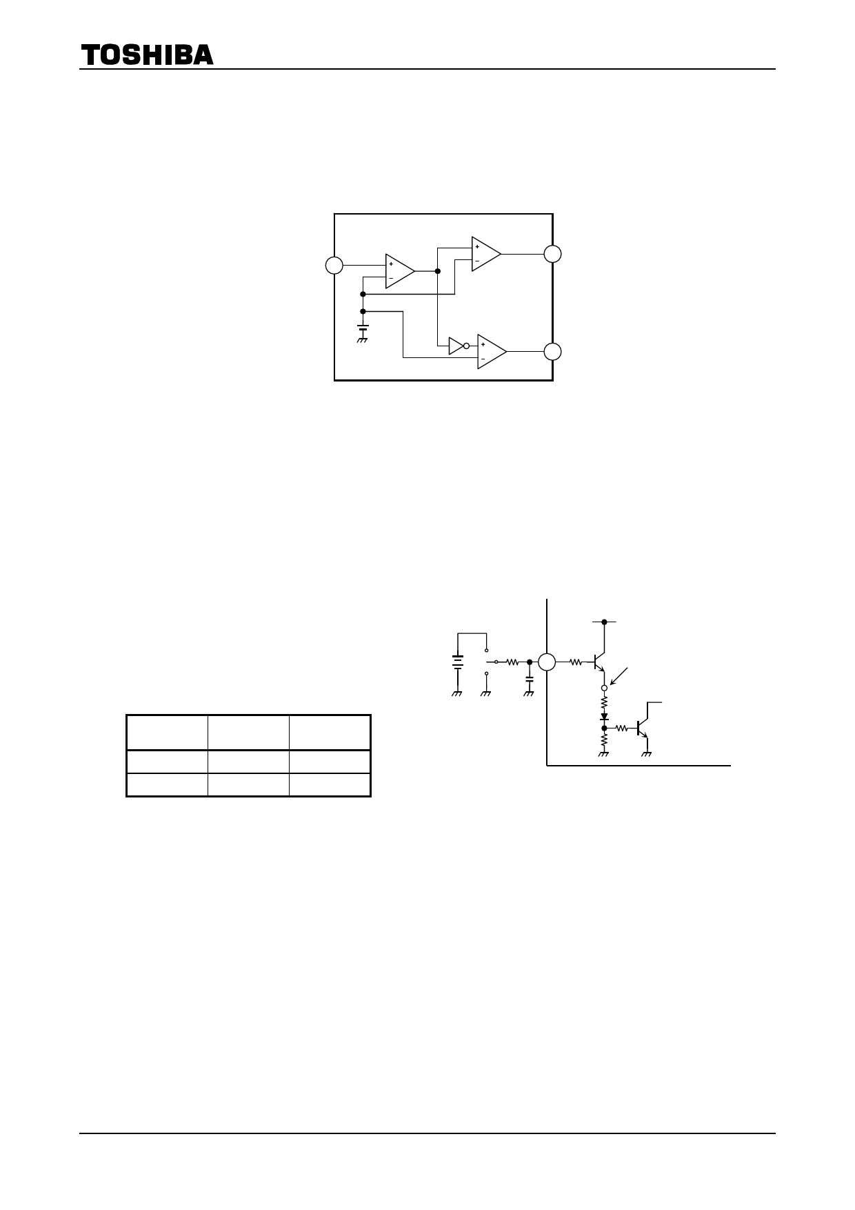
Input
Amp. 1
Amp. 2A
Amp. 2B
Figure 1 Block Diagram
The voltage gain of amp.1
: GV1 = 8dB
The voltage gain of amp.2A, B : GV2 = 20dB
The voltage gain of BTL connection: GV (BTL) = 6dB
Therefore, the total voltage gain is decided by expression below.
GV = GV1 + GV2 + GV (BTL) = 8 + 20 + 6 = 34dB
2. Standby SW Function (pin 1)
By means of controlling pin 1 (standby pin) to
High and Low, the power supply can be set to ON
and OFF. The threshold voltage of pin 1 is set at
about 3 VBE (typ.), and the power supply current is
about 2 μA (typ.) in the standby state.
Control Voltage of Pin 4: VSB
Stand-by
ON
OFF
Power
OFF
ON
VSB (V)
0 to 0.5
2.5 to 6
When changing the time constant of pin 1, check the
pop noise.
ON Power
OFF
10 kΩ
1
VCC
≈ 2 VBE
to BIAS
CUTTING CIRCUIT
Figure 2 With pin 1 set to High,
Power is turned ON
Advantage of Standby SW
(1) Since VCC can directly be controlled to ON or OFF by the microcomputer, the switching relay can be
omitted.
(2) Since the control current is microscopic, the switching relay of small current capacity is satisfactory
for switching.
3
2007-02-20
Share Link: 