TC1026 View Datasheet(PDF) - Microchip Technology
Part Name
Description
Manufacturer
TC1026
Microchip Technology

TC1026 Datasheet PDF : 18 Pages
| |||
TC1026
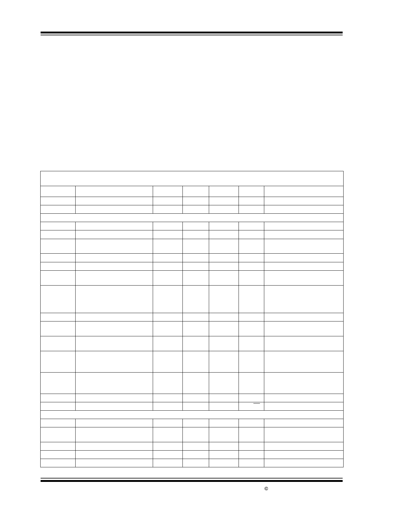
1.0 ELECTRICAL
CHARACTERISTICS
ABSOLUTE MAXIMUM RATINGS*
Supply Voltage ......................................................6.0V
Package Power Dissipation:
8-Pin PDIP ...............................................730 mW
8-Pin SOIC ...............................................470 mW
8-Pin MSOP .............................................320 mW
Voltage on Any Pin .......... (VSS – 0.3V) to (VDD + 0.3V)
Junction Temperature....................................... +150°C
Operating Temperature Range............. -40°C to +85°C
Storage Temperature Range .............. -55°C to +150°C
*Stresses above those listed under "Absolute Maximum
Ratings" may cause permanent damage to the device. These
are stress ratings only and functional operation of the device
at these or any other conditions above those indicated in the
operation sections of the specifications is not implied.
Exposure to Absolute Maximum Rating conditions for
extended periods may affect device reliability.
TC1026 ELECTRICAL SPECIFICATIONS
Electrical Characteristics: Typical values apply at 25°C and VDD = 3.0V; TA = -40° to +85°C, and VDD = 1.8V to 5.5V, unless
otherwise specified.
Symbol
Parameter
Min
Typ
Max
Units
Test Conditions
VDD
IQ
Op Amp
AVOL
VICMR
VOS
Supply Voltage
Supply Current
Large Signal Voltage Gain
Common Mode Input Range
Input Offset Voltage
IB
VOS (DRIFT)
GBWP
Input Bias Current
Input Offset Voltage Drift
Gain-Bandwidth Product
SR
Slew Rate
1.8
—
—
VSS – 0.2
-100
—
—
—
VOUT
CMRR
PSRR
ISRC
Output Signal Swing
VSS + 0.05
Common Mode Rejection Ratio
66
Power Supply Rejection Ratio
80
Output Source Current
3
ISINK
Output SInk Current
—
En
en
Comparator
VIR
VOS
Input Noise Voltage
Input Noise Voltage Density
Input Voltage Range
Input Offset Voltage
IB
Input Bias Current
VOH
Output High Voltage
VOL
Output Low Voltage
—
—
VSS – 0.2
-5
-5
––
VDD – 0.3
—
—
12
100
—
±100
±0.3
50
±4
90
35
—
—
—
—
125
10
125
—
—
—
—
—
—
5.5
V
18
µA All outputs unloaded
—
VDD + 0.2
±500
±1.5
100
—
—
—
VDD – 0.05
—
—
—
—
—
V/mV
V
µV
mV
pA
µV/°C
kHz
mV/µsec
V
dB
dB
mA
nV/Hz
µVpp
RL = 10kΩ, VDD = 5V
VDD = 3V, VCM = 1.5V, TA = 25°C
TA = -40°C to 85°C
TA = 25°C, VCM = VDD to VSS
VDD = 3V, VCM = 1.5V
VDD = 1.8V to 5.5V;
VO = VDD to VSS
CL = 100pF
RL = 1MΩ to GND
Gain = 1
VIN = VSS to VDD
RL = 10kΩ
TA = 25°C, VDD = 5V
VCM = VDD to VSS
TA = 25°C, VCM = VSS
VDD = 1.8V to 5V
VIN+ = VDD, VIN- = VSS
Output Shorted to VSS
VDD = 1.8V, Gain = 1
IN+ = VSS, IN- = VDD
Output Shorted to VDD
VDD = 1.8V, Gain = 1
0.1Hz to 10Hz
—
nV/√Hz 1kHz
VDD + 0.2
+5
+5
±100
—
0.3
V
mV VDD = 3V, TA = 25°C
TA = -40°C to 85°C
pA TA = 25°C, IN+ = VDD to VSS
V
RL = 10kΩ to VSS
V
RL = 10kΩ to VDD
DS21725B-page 2
© 2002 Microchip Technology Inc.
Share Link: