TC4423A View Datasheet(PDF) - Microchip Technology
Part Name
Description
Manufacturer
TC4423A Datasheet PDF : 22 Pages
| |||
TC4423A/TC4424A/TC4425A
1.0 ELECTRICAL
CHARACTERISTICS
Absolute Maximum Ratings †
Supply Voltage ................................................................+20V
Input Voltage, IN A or IN B .......... (VDD + 0.3V) to (GND – 5V)
Package Power Dissipation (TA=50°C)
8L PDIP .......................................................................1.2W
8L SOIC.................................................................... 0.61W
16L SOIC.....................................................................1.1W
8L DFN .................................................................... Note 3
† Notice: Stresses above those listed under "Maximum
Ratings" may cause permanent damage to the device. This is
a stress rating only and functional operation of the device at
those or any other conditions above those indicated in the
operational sections of this specification is not intended.
Exposure to maximum rating conditions for extended periods
may affect device reliability.
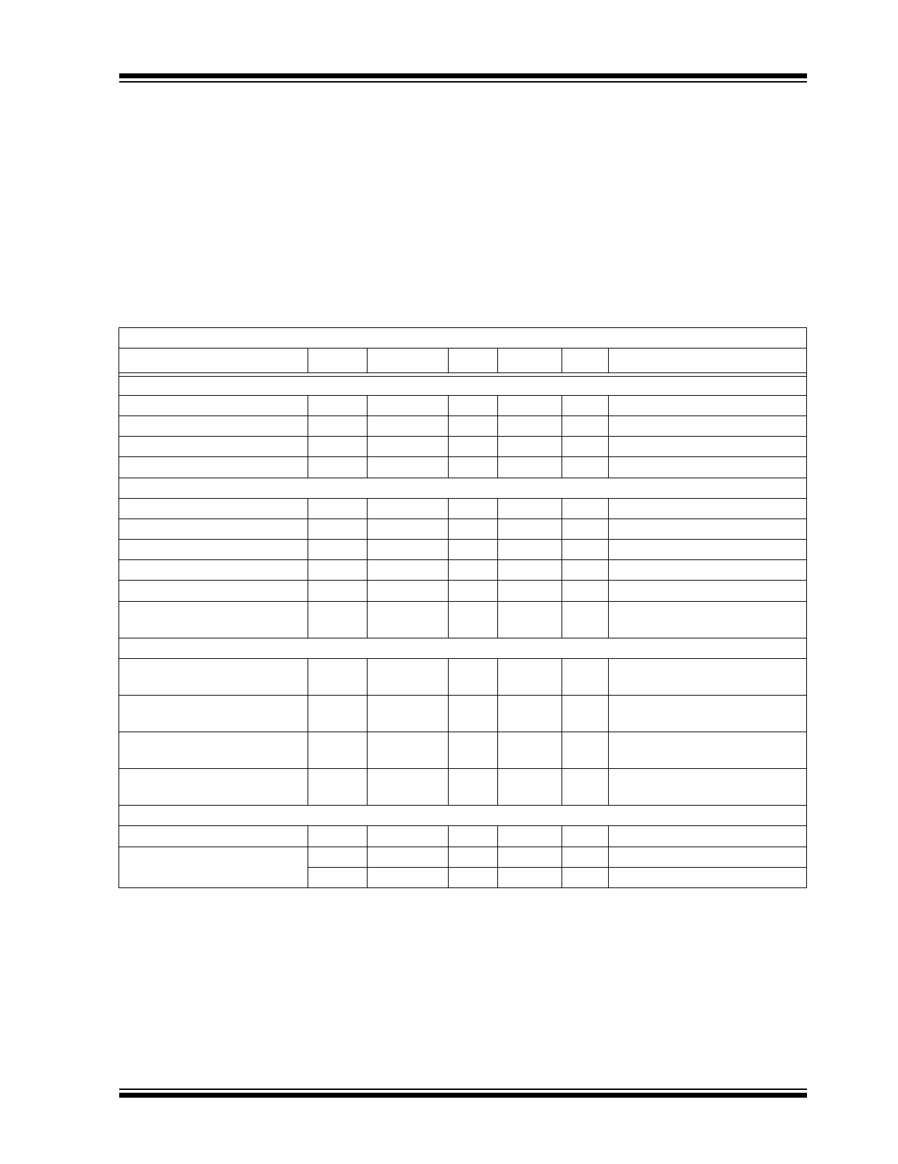
DC CHARACTERISTICS (NOTE 2)
Electrical Specifications: Unless otherwise indicated, TA = +25°C, with 4.5V ≤ VDD ≤ 18V.
Parameters
Sym
Min
Typ Max Units
Conditions
Input
Logic ‘1’, High Input Voltage
VIH
Logic ‘0’, Low Input Voltage
VIL
Input Current
IIN
Input Voltage
VIN
Output
2.4
1.5
—
V
—
1.3
0.8
V
–1
—
1
µA 0V ≤ VIN ≤ VDD
-5
— VDD+0.3 V
High Output Voltage
Low Output Voltage
Output Resistance, High
Output Resistance, Low
Peak Output Current
Latch-Up Protection With-
stand Reverse Current
VOH
VOL
ROH
ROL
IPK
IREV
VDD – 0.025
—
—
—
—
—
—
—
2.2
2.8
4.5
>1.5
—
0.025
3.0
3.5
—
—
V DC Test
V DC Test
Ω IOUT = 10 mA, VDD = 18V
Ω IOUT = 10 mA, VDD = 18V
A 10V≤ VDD ≤18V (Note 2)
A Duty cycle ≤ 2%, t ≤ 300 µsec.
Switching Time (Note 1)
Rise Time
Fall Time
Delay Time
Delay Time
Power Supply
tR
—
12
21
ns Figure 4-1, Figure 4-2,
CL = 1800 pF
tF
—
12
21
ns Figure 4-1, Figure 4-2,
CL = 1800 pF
tD1
—
40
48
ns Figure 4-1, Figure 4-2,
CL = 1800 pF
tD2
—
41
48
ns Figure 4-1, Figure 4-2,
CL = 1800 pF
Supply Voltage
VDD
4.5
Power Supply Current
IS
—
IS
—
Note 1: Switching times ensured by design.
—
18
V
1.0
2.0
mA VIN = 3V (Both inputs)
0.15
0.25
mA VIN = 0V (Both inputs)
2: Tested during characterization, not production tested.
3: Package power dissipation is dependent on the copper pad area on the PCB.
© 2007 Microchip Technology Inc.
DS21998B-page 3
Share Link: 