TC647(2002) View Datasheet(PDF) - Microchip Technology
Part Name
Description
Manufacturer
TC647 Datasheet PDF : 28 Pages
| |||
TC647
1.0 ELECTRICAL
CHARACTERISTICS
Absolute Maximum Ratings*
Supply Voltage ......................................................... 6V
Input Voltage, Any Pin.... (GND – 0.3V) to (VDD +0.3V)
Package Thermal Resistance:
PDIP (RθJA)............................................. 125°C/W
SOIC (RθJA) ............................................ 155°C/W
MSOP (RθJA) .......................................... 200°C/W
Specified Temperature Range ........... -40°C to +125°C
Storage Temperature Range.............. -65°C to +150°C
*Stresses above those listed under "Absolute Maximum Rat-
ings" may cause permanent damage to the device. These are
stress ratings only and functional operation of the device at
these or any other conditions above those indicated in the
operation sections of the specifications is not implied. Expo-
sure to absolute maximum rating conditions for extended peri-
ods may affect device reliability.
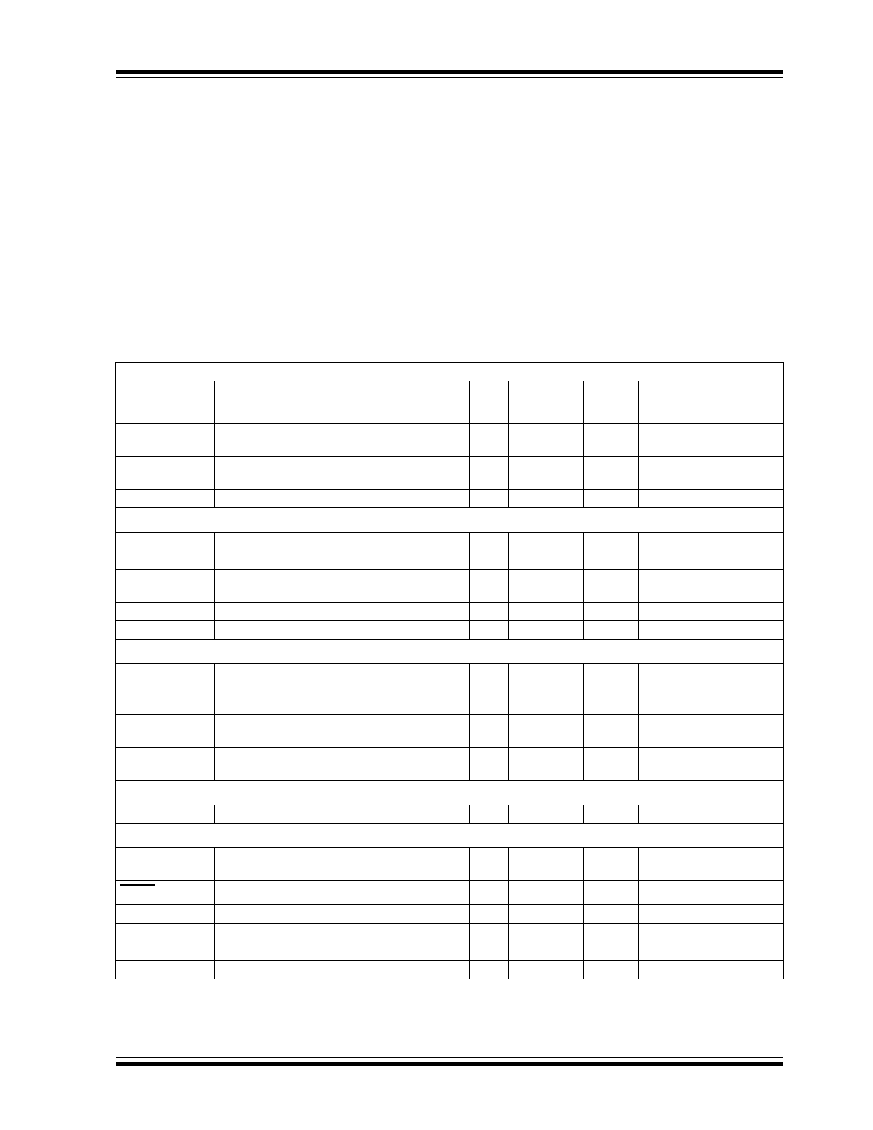
DC ELECTRICAL SPECIFICATIONS
Electrical Characteristics: Unless otherwise specified, TMIN < TA < TMAX, VDD = 3.0V to 5.5V.
Symbol
Parameter
Min
Typ
Max
Units
VDD
Supply Voltage
3.0
—
5.5
V
IDD
Supply Current, Operating
—
0.5
1
mA
IDD(SHDN)
IIN
VOUT Output
tR
tF
tSHDN
IOL
IOH
VIN, VMIN Inputs
VC(MAX)
VC(SPAN)
VSHDN
VREL
Supply Current,
Shutdown Mode
VIN, VMIN Input Leakage
VOUT Rise Time
VOUT Fall Time
Pulse Width (On VMIN) to Clear
Fault Mode
Sink Current at VOUT Output
Source Current at VOUT Output
Input Voltage at VIN or VMIN for
100% PWM Duty Cycle
VC(MAX) - VC(MIN)
Voltage Applied to VMIN to
Ensure Shutdown Mode
Voltage Applied to VMIN to
Release Shutdown Mode
Pulse Width Modulator
FPWM
SENSE Input
PWM Frequency
VTH(SENSE)
SENSE Input Threshold
Voltage with Respect to GND
FAULT Output
VOL
tMP
tSTARTUP
tDIAG
Note 1:
Output Low Voltage
Missing Pulse Detector Timer
Start-up Timer
Diagnostic Timer
Ensured by design, not tested.
—
25
—
µA
– 1.0
—
+1.0
µA
—
—
50
µsec
—
—
50
µsec
30
—
—
µsec
1.0
—
—
mA
5.0
—
—
mA
2.5
2.65
2.8
V
1.3
1.4
1.5
V
—
— VDD x 0.13
V
VDD x 0.19 —
—
V
26
30
34
Hz
50
70
90
mV
—
—
0.3
V
—
32/F
—
Sec
—
32/F
—
Sec
—
3/F
—
Sec
Test Conditions
Pins 6, 7 Open,
CF = 1 µF, VIN = VC(MAX)
Pins 6, 7 Open,
CF = 1 µF, VMIN = 0.35V
Note 1
IOH = 5 mA, Note 1
IOL = 1 mA, Note 1
VSHDN, VHYST
Specifications, Note 1
VOL = 10% of VDD
VOH = 80% of VDD
VDD = 5V
CF = 1.0 µF
Note 1
IOL = 2.5 mA
2002 Microchip Technology Inc.
DS21447C-page 3
Share Link: 