TC7116 View Datasheet(PDF) - TelCom Semiconductor Inc => Microchip
Part Name
Description
Manufacturer
TC7116 Datasheet PDF : 14 Pages
| |||
TC7116
TC7116A
TC7117
TC7117A
3-1/2 DIGIT ANALOG-TO-DIGITAL
CONVERTERS WITH HOLD
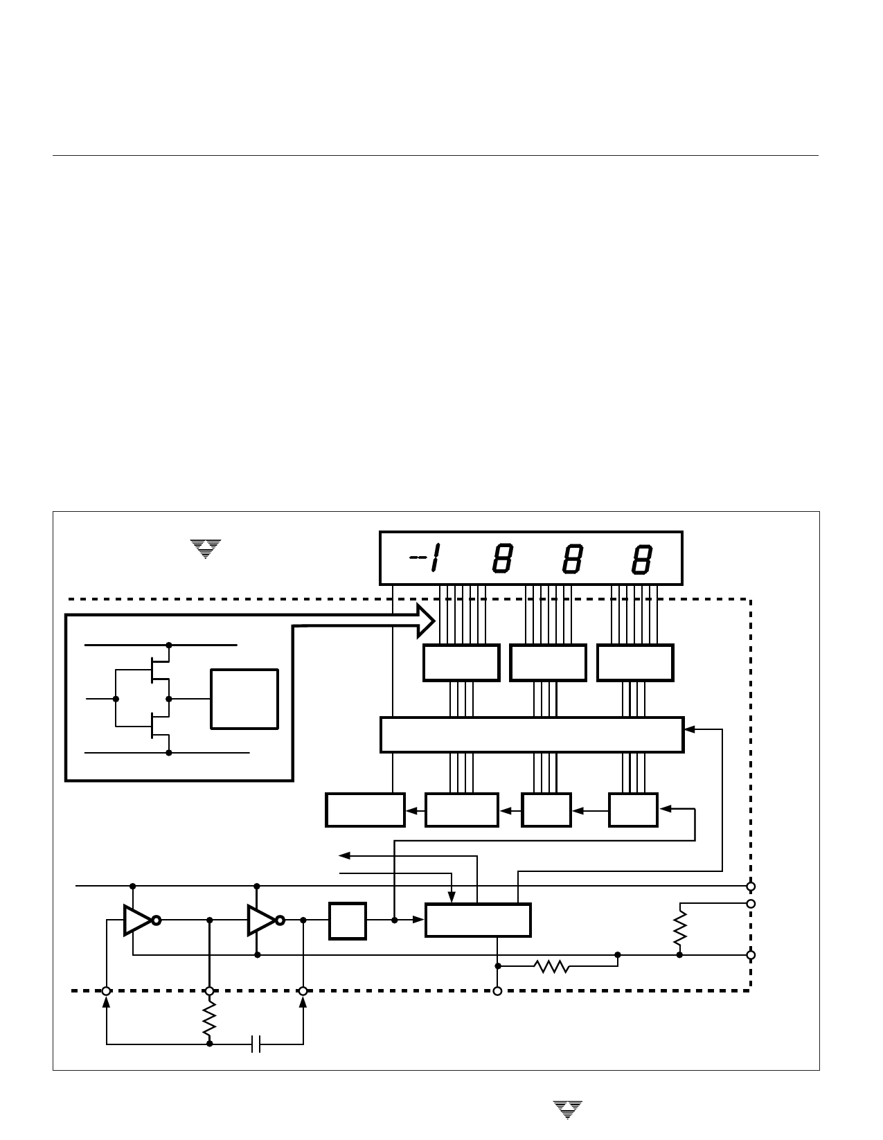
System Timing
The clocking method used for the TC7116/TC7116A
and TC7117/TC7117A is shown in Figure 9. Three clocking
methods may be used:
(1) An external oscillator connected to pin 40.
(2) A crystal between pins 39 and 40.
(3) An RC network using all three pins.
The oscillator frequency is Ϭ 4 before it clocks the
decade counters. It is then further divided to form the three
convert-cycle phases: signal integrate (1000 counts), refer-
ence deintegrate (0 to 2000 counts), and auto-zero (1000 to
3000 counts). For signals less than full scale, auto-zero gets
the unused portion of reference deintegrate. This makes a
complete measure cycle of 4000 (16,000 clock pulses)
independent of input voltage. For 3 readings per second, an
oscillator frequency of 48 kHz would be used.
To achieve maximum rejection of 60-Hz pickup, the
signal-integrate cycle should be a multiple of 60 Hz. Oscil-
lator frequencies of 240 kHz, 120 kHz, 80 kHz, 60 kHz, 48
kHz, 40 kHz, etc. should be selected. For 50 Hz rejection,
oscillator frequencies of 200 kHz, 100 kHz, 66-2/3 kHz, 50
kHz, 40 kHz, etc. would be suitable. Note that 40 kHz (2.5
readings per second) will reject both 50 Hz and 60 Hz.
HOLD Reading Input
When HLDR is at a logic HIGH the latch will not be
updated. Analog-to-digital conversions will continue but will
not be updated until HLDR is returned to LOW. To continu-
ously update the display, connect to test (TC7116/TC7116A)
or ground (TC7117/TC7117A), or disconnect. This input is
CMOS compatible with 70 kΩ typical resistance to TEST
(TC7116/TC7116A) or ground (TC7117/TC7117A).
TC7117
TC7117A
TYPICAL SEGMENT OUTPUT
V+
0.5 mA
8 mA
TO
SEGMENT
DIGITAL GROUND
7-SEGMENT 7-SEGMENT 7-SEGMENT
DECODE
DECODE
DECODE
LATCH
THOUSANDS HUNDREDS
TENS
UNITS
TO SWITCH DRIVERS
V+ FROM COMPARATOR OUTPUT
CLOCK
÷4
40
OSC 1
39
OSC2
38
OSC 3
CONTROL LOGIC
1
~70 kΩ
HLDR
35 V+
37
TEST
500Ω
21 DIGITAL
GND
3-212
Figure 9. TC7117/TC7117A Digital Section
TELCOM SEMICONDUCTOR, INC.
Share Link: 