TC7116 View Datasheet(PDF) - TelCom Semiconductor Inc => Microchip
Part Name
Description
Manufacturer
TC7116 Datasheet PDF : 14 Pages
| |||
TC7116
TC7116A
TC7117
TC7117A
3-1/2 DIGIT ANALOG-TO-DIGITAL
CONVERTERS WITH HOLD
ABSOLUTE MAXIMUM RATINGS*
Supply Voltage
TC7116/TC7116A: V+ to V– ................................. 15V
TC7117/TC7117A: V+ to GND ............................. +6V
V– to GND ............................ – 9V
Analog Input Voltage (Either Input) (Note 1) ........ V+ to V–
Reference Input Voltage (Either Input) ................. V+ to V–
Clock Input
TC7116/TC7116A ..................................... TEST to V+
TC7117/TC7117A ...................................... GND to V+
Package Power Dissipation, TA ≤ 70°C (Note 2)
CerDIP ..............................................................2.29W
Plastic DIP ........................................................1.23W
Plastic Chip Carrier (PLCC) ..............................1.23W
Plastic Quad Flat Package (PQFP) ..................1.00W
Operating Temperature
“C” Device .............................................. 0°C to +70°C
“I” Device .......................................... – 25°C to +85°C
Storage Temperature ............................ – 65°C to +150°C
Lead Temperature (Soldering, 10 sec) ................. +300°C
*Static-sensitive device. Unused devices must be stored in conductive
material. Protect devices from static discharge and static fields. Stresses
above those listed under Absolute Maximum Ratings may cause perma-
nent damage to the device. These are stress ratings only and functional
operation of the device at these or any other conditions above those
indicated in the operational sections of the specifications is not implied.
Exposure to Absolute Maximum Rating Conditions for extended periods
may affect device reliability.
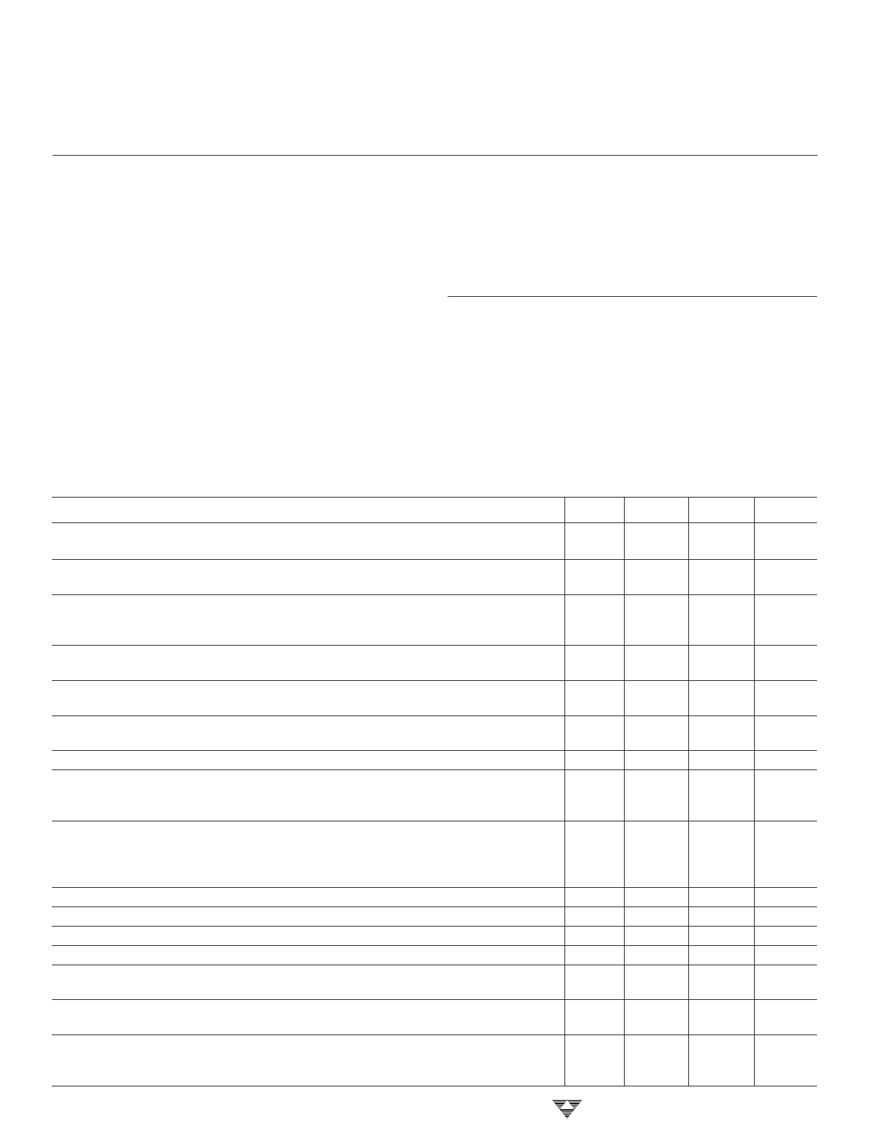
ELECTRICAL CHARACTERISTICS (Note 3)
Parameter
Test Conditions
Zero Input Reading
Ratiometric Reading
Roll-Over Error (Difference in
Reading for Equal Positive and
Negative Readings Near Full Scale)
Linearity (Maximum Deviation From
Best Straight Line Fit)
Common-Mode Rejection Ratio (Note 4)
Noise (Peak-to-Peak Value Not
Exceeded 95% of Time)
Leakage Current at Input
Zero Reading Drift
Scale Factor Temperature Coefficient
Input Resistance, Pin 1
VIL, Pin 1
VIL, Pin 1
VIH, Pin 1
Supply Current (Does Not Include
LED Current for 7117/A)
Analog Common Voltage
(With Respect to Positive Supply)
Temperature Coefficient of Analog Common
(With Respect to Positive Supply)
VIN = 0V
Full Scale = 200 mV
VIN = VREF
VREF = 100 mV
–VIN = +VIN ≅ 200 mV or ≈ 2V
Full Scale = 200 mV or 2V
VCM = ±1V, VIN = 0V
Full Scale = 200 mV
VIN = 0V
Full Scale = 200 mV
VIN = 0V
VIN = 0V
“C” Device: 0°C to +70°C
“I” Device: –25°C to +85°C
VIN = 199 mV
“C” Device: 0°C to +70°C
(Ext Ref = 0 ppm/°C)
“I” Device: –25°C to +85°C
Note 6
TC7116/A Only
TC7117/A Only
Both
VIN = 0V
25 kΩ Between Common
and Positive Supply
"C" Device: 0°C to +70°C
TC7116A/TC7117A
TC7116/TC7117
3-204
Min Typ
Max
—
±0
—
999 999/1000 1000
–1
±0.2
+1
Unit
Digital
Reading
Digital
Reading
Counts
–1
±0.2
+1
Counts
—
50
—
µV/V
—
15
—
µV
—
1
10
pA
—
0.2
—
1
1
µV/°C
2
µv/°C
—
1
5
ppm/°C
—
—
20
ppm/°C
30
70
—
kΩ
—
— Test +1.5 V
—
— GND +1.5 V
V + – 1.5 —
—
V
—
0.8
1.8
mA
2.4
3.05
3.35 V
—
20
—
80
50
ppm/°C
—
ppm/°C
TELCOM SEMICONDUCTOR, INC.
Share Link: 