TC7116 View Datasheet(PDF) - TelCom Semiconductor Inc => Microchip
Part Name
Description
Manufacturer
TC7116 Datasheet PDF : 14 Pages
| |||
3-1/2 DIGIT ANALOG-TO-DIGITAL
CONVERTERS WITH HOLD
1 TC7116
TC7116A
TC7117
TC7117A
C
+
REF
V+
CREF
VR+ EF
34 36
C R– EF
33
10 µA
V
+
IN
31
INT
A/Z
ANALOG 32
COMMON
V
–
IN
30
INT
A/Z
DE
DE
(–)
(+)
A/Z
DE (+) DE (–)
A/Z & DE (±)
RINT
VBUFF
V+
28 35
–
+
–
+
LOW
TEMP
DRIFT
ZENER
VREF
V+ –3V
26
V–
CAZ
AUTO-
ZERO
29
CINT
VINT
27
INTEGRATOR
–
+
+
COMPARATOR
TC7116
TC7116A
TC7117
TC7117A
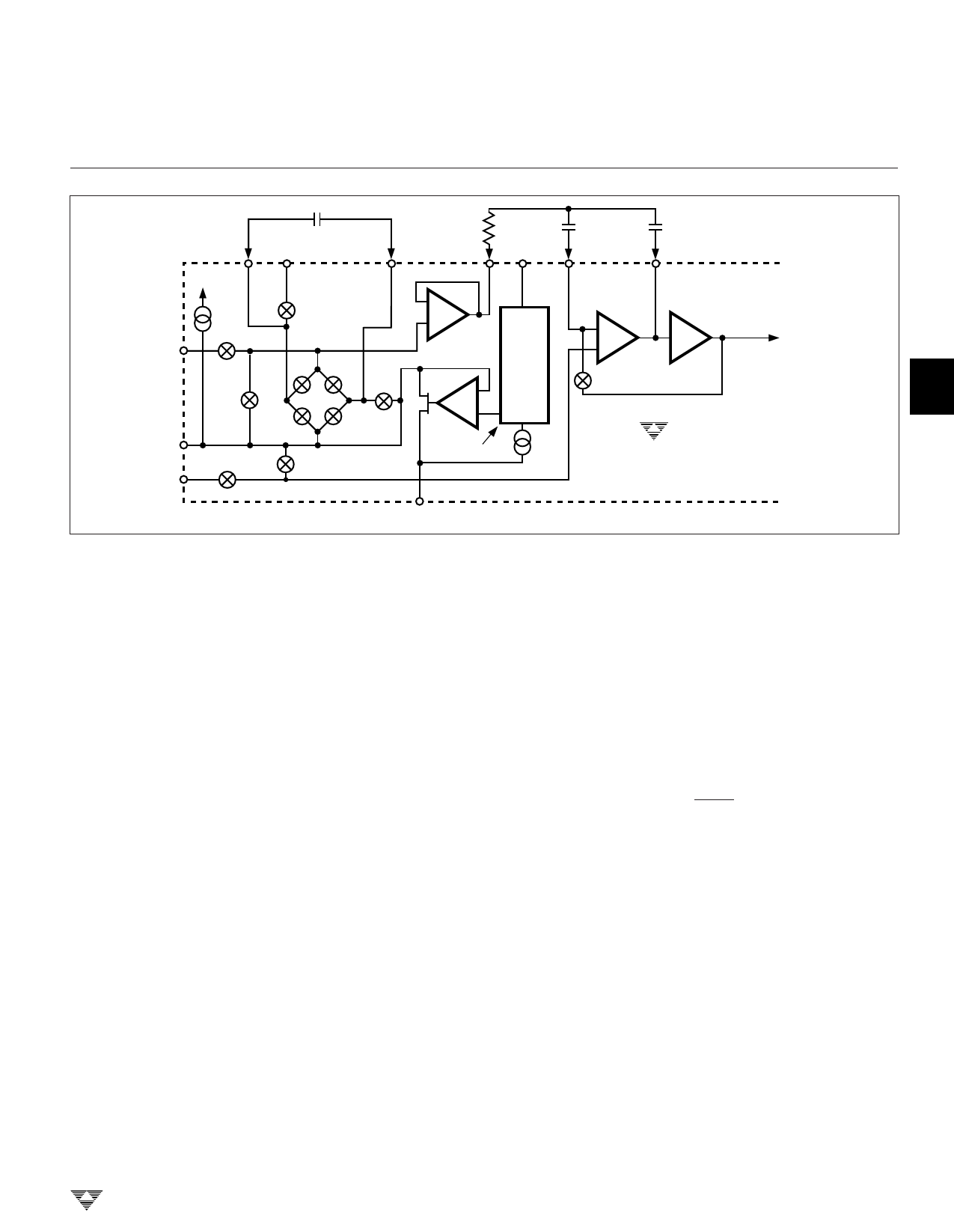
Figure 3. Analog Section of TC7116/TC7116A and TC7117/TC7117A
TO
DIGITAL
SECTION
2
3
4
ANALOG SECTION
(All Pin designations refers to 40-Pin Dip)
Figure 3 shows the block diagram of the analog section
for the TC7116/TC7116A and TC7117/TC7117A. Each
measurement cycle is divided into three phases: (1) auto-
zero (A-Z), (2) signal integrate (INT), and (3) reference
integrate (REF) or deintegrate (DE).
Auto-Zero Phase
High and low inputs are disconnected from the pins
and internally shorted to analog common. The reference
capacitor is charged to the reference voltage. A feedback
loop is closed around the system to charge the auto-zero
capacitor (CAZ) to compensate for offset voltages in the
buffer amplifier, integrator, and comparator. Since the com-
parator is included in the loop, A-Z accuracy is limited only
by system noise. The offset referred to the input is less
than 10 µV.
Signal-Integrate Phase
The auto-zero loop is opened, the internal short is
removed, and the internal high and low inputs are con-
nected to the external pins. The converter then integrates
the
differential
voltages
between
V+IN
and
V
–
IN
for
a
fixed
time. This differential voltage can be within a wide com-
mon-mode range; 1V of either supply. However, if the input
signal has no return with respect to the converter power
supply,
V
–
IN
can
be
tied
to
analog
common
to
establish
the
correct common-mode voltage. At the end of this phase,
the polarity of the integrated signal is determined.
TELCOM SEMICONDUCTOR, INC.
Reference Integrate Phase
The final phase is reference integrate, or deintegrate.
Input low is internally connected to analog common and
input high is connected across the previously charged
5 reference capacitor. Circuitry within the chip ensures that
the capacitor will be connected with the correct polarity to
cause the integrator output to return to zero. The time
required for the output to return to zero is proportional to
the input signal. The digital reading displayed is:
1000 ×
VIN .
VREF
Reference
6
The positive reference voltage (V+REF) is referred to
analog common.
Differential Input
This input can accept differential voltages anywhere
within the common-mode range of the input amplifier or,
7 specifically, from 1V below the positive supply to 1V above
the negative supply. In this range, the system has a CMRR
of 86 dB, typical. However, since the integrator also swings
with the common-mode voltage, care must be exercised to
ensure that the integrator output does not saturate. A
worst- case condition would be a large, positive common-
mode voltage with a near full-scale negative differential
input voltage. The negative-input signal drives the integra-
8 tor positive when most of its swing has been used up by the
positive common-mode voltage. For these critical applica-
tions, the integrator swing can be reduced to less than the
3-209
Share Link: 