TC7126 View Datasheet(PDF) - TelCom Semiconductor Inc => Microchip
Part Name
Description
Manufacturer
TC7126 Datasheet PDF : 13 Pages
| |||
TC7126
TC7126A
3-1/2 DIGIT
ANALOG-TO-DIGITAL CONVERTERS
SEGMENT
DRIVE
LCD
MEASURED
SYSTEM
V+
V–
GND
V+ V– GND
POWER
SOURCE
VBUFF
VI+N
CAZ VINT
VI–N
TC7126A
ANALOG
COMMON
VR–EF
VR+ EF
V+
POL BP
OSC1
OSC3
OV –SC2
+
9V
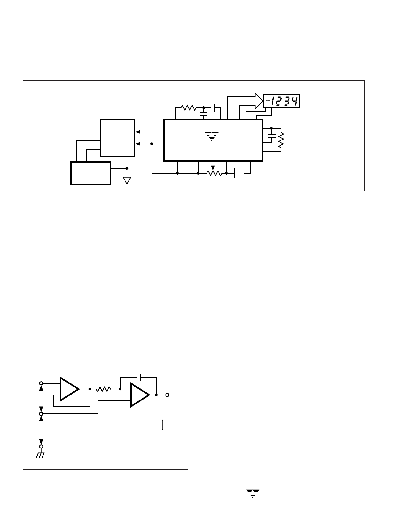
Figure 5. Common-Mode Voltage Removed in Battery Operation With VIN = Analog Common
100 µA. This FET will hold the common line at 3V should an
external load attempt to pull the common line toward V+.
Analog common source current is limited to 1 µA. Therefore,
analog common is easily pulled to a more negative voltage
(i.e., below V+ – 3V).
The TC7126A connects the internal V+IN and VI–N in-
puts to analog common during the auto-zero phase. During
the reference-integrate phase, VI–N is connected to analog
common. If V+IN is not externally connected to analog com-
mon, a common-mode voltage exists, but is rejected by the
converter's 86 dB common-mode rejection ratio. In battery
operation, analog common and VI–N are usually connected,
removing common-mode voltage concerns. In systems where
VI–N is connected to power supply ground or to a given
voltage, analog common should be connected to VI–N.
The analog common pin serves to set the analog sec-
tion reference, or common point. The TC7126A is specifi-
cally designed to operate from a battery or in any measure-
ment system where input signals are not referenced (float)
+
VIN
–
VCM
INPUT
BUFFER
+
RI
–
CI
–
+
VI
INTEGRATOR
[ VI
Where:
=
TI
RI CI
VCM – VIN
TI
=
Integration time
=
4000
fOSC
CI = Integration capacitor
RI = Integration resistor
Figure 6. Common-Mode Voltage Reduces Available Integrator
Swing (VCOM ≠ VIN)
with respect to the TC7126A's power source. The analog
common potential of V+ –3V gives a 7V end of battery life
voltage. The common potential has a 0.001%/% voltage
coefficient and a 15Ω output impedance.
With sufficiently high total supply voltage (V+–V– >7V),
analog common is a very stable potential with excellent
temperature stability (typically 35 ppm/°c). This potential
can be used to generate the TC7126A's reference voltage.
An external voltage reference will be unnecessary in most
cases because of the 35 ppm/°C temperature coefficient.
See "TC7126A Internal Voltage Reference" discussion.
TEST (Pin 37)
The TEST pin potential is 5V less than V+. TEST may be
used as the negative power supply connection for external
CMOS logic. The TEST pin is tied to the internally-generated
negative logic supply through a 500Ω resistor. The TEST pin
load should not be more than 1 mA. See "Digital Section" for
additional information on using TEST as a negative digital
logic supply.
If TEST is pulled HIGH (to V+), all segments plus the
minus sign will be activated. DO NOT OPERATE IN THIS
MODE FOR MORE THAN SEVERAL MINUTES. With
TEST= V+, the LCD segments are impressed with a DC
voltage which will destroy the LCD.
TC7126A Internal Voltage Reference
The TC7126A's analog common voltage temperature
stability has been significantly improved (Figure 7). The "A"
version of the industry-standard TC7126 device allows
users to upgrade old systems and design new systems
without external voltage references. External R and C val-
ues do not need to be changed. Figure 10 shows analog
common supplying the necessary voltage reference for the
TC7126A.
3-226
TELCOM SEMICONDUCTOR, INC.
Share Link: 