TC7126 View Datasheet(PDF) - TelCom Semiconductor Inc => Microchip
Part Name
Description
Manufacturer
TC7126 Datasheet PDF : 13 Pages
| |||
TC7126
TC7126A
3-1/2 DIGIT
ANALOG-TO-DIGITAL CONVERTERS
ABSOLUTE MAXIMUM RATINGS*
Supply Voltage (V+ to V–)......................................... +15V
Analog Input Voltage (Either Input) (Note 1) ........ V+ to V–
Reference Input Voltage (Either Input) ................. V+ to V–
Clock Input ...................................................... TEST to V+
Operating Temperature Range
C Devices .............................................. 0°C to +70°C
I Devices ........................................... – 25°C to +85°C
Storage Temperature Range ................ – 65°C to +150°C
Lead Temperature (Soldering, 10 sec) ................. +300°C
Power Dissipation, (TA ≤ 70°C), (Note 2)
44-Pin PQFP .................................................... 1.00W
44-Pin PLCC .....................................................1.23W
40-Pin Plastic PDIP .......................................... 1.23W
*Static-sensitive device. Unused devices must be stored in conductive
material. Protect devices from static discharge and static fields. Stresses
above those listed under Absolute Maximum Ratings may cause perma-
nent damage to the device. These are stress ratings only and functional
operation of the device at these or any other conditions above those
indicated in the operational sections of the specifications is not implied.
Exposure to Absolute Maximum Rating Conditions for extended periods
may affect device reliability.
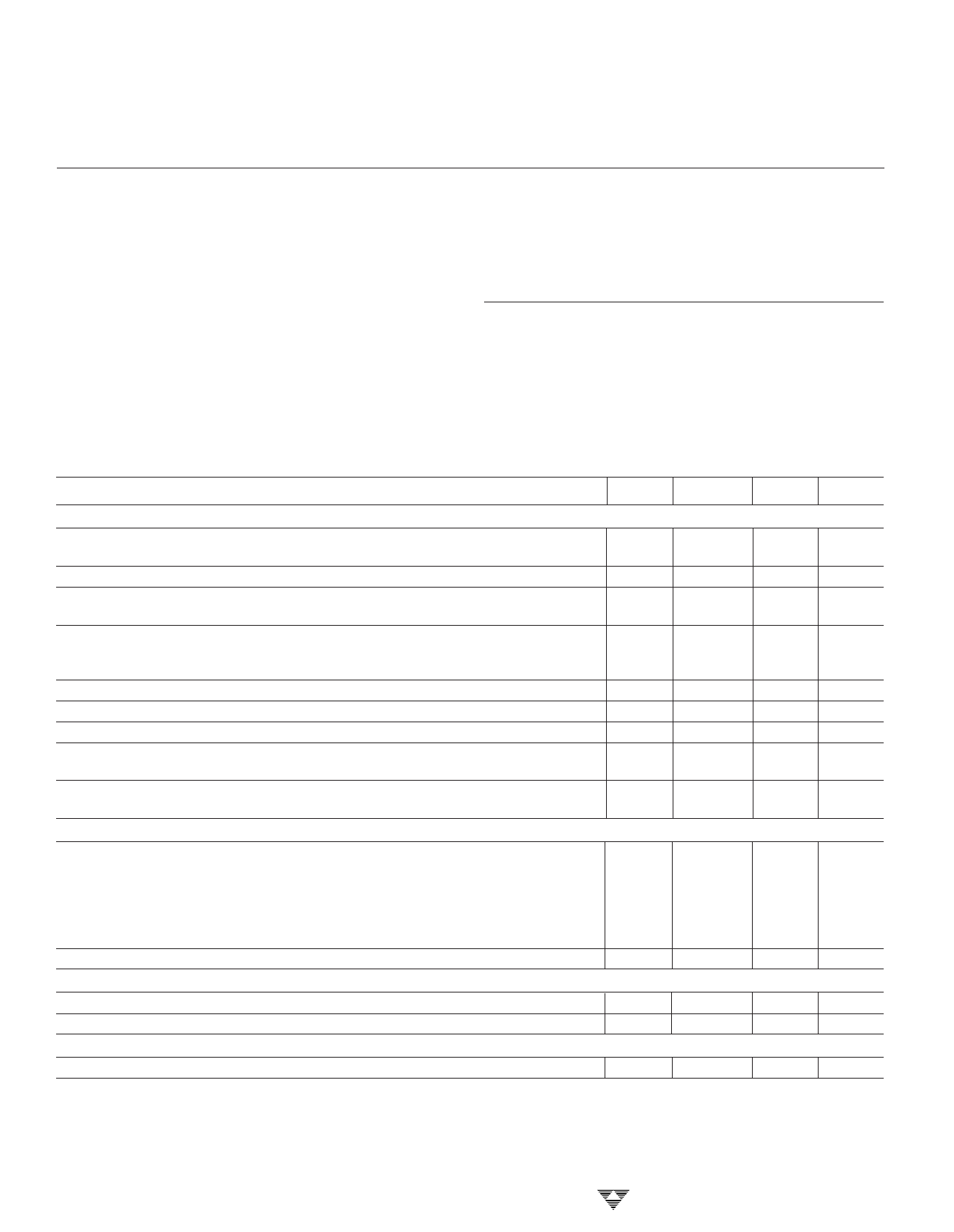
ELECTRICAL CHARACTERISTICS: VS = +9V, fCLK = 16 kHz, and TA = +25°C, unless otherwise noted.
Symbol Parameter
Test Conditions
Min
Typ
Max Unit
Input
Zero Input Reading
VIN = 0V
Full Scale = 200 mV
–000.0 ±000.0 +000.0 Digital
Reading
Zero Reading Drift
Ratiometric Reading
VIN = 0V, 0°C ≤ TA ≤ +70°C
VIN = VREF, VREF = 100 mV
—
0.2
1
µV/°C
999 999/1000 1000 Digital
Reading
NL
Linearity Error
Full Scale = 200 mV or 2V
Max Deviation From Best Fit
Straight Line
–1
±0.2
1
Count
eN
IL
CMRR
Roll-Over Error
Noise
Input Leakage Current
Common-Mode Rejection
Ratio
–VIN = +VIN ≈ 200 mV
VIN = 0V, Full Scale = 200 mV
VIN = 0V
VCM = ±1V, VIN = 0V,
Full Scale = 200 mV
–1
±0.2 1 Count
—
15
—
µVP-P
—
1
10
pA
—
50
—
µV/V
Scale Factor Temperature
Coefficient
VIN = 199 mV, 0°C ≤ TA ≤ +70°C
—
1
Ext Ref Temp Coeff = 0 ppm/°C
5
ppm/°C
Analog Common
VCTC
Analog Common
Temperature Coefficient
VC
Analog Common Voltage
250 kΩ Between Common and V+
—
—
—
—
0°C ≤ TA ≤ +70°C ("C" Devices):
TC7126
—
—
—
—
—
80
—
ppm/°C
TC7126A
—
35
75
ppm/°C
– 25°C ≤ TA ≤ +85°C ("I" Device):
TC7126A
—
35
100
ppm/°C
250 kΩ Between Common and V+
2.7
3.05
3.35 V
LCD Drive
VSD
VBD
LCD Segment Drive Voltage
LCD Backplane Drive Voltage
V+ to V– = 9V
V+ to V– = 9V
4
5
6
VP-P
4
5
6
VP-P
Power Supply
IS
Power Supply Current
VIN = 0V, V+ to V– = 9V (Note 6)
—
55
100 µA
NOTES: 1. Input voltage may exceed supply voltages when input current is limited to 100 µA.
2. Dissipation rating assumes device is mounted with all leads soldered to PC board.
3. Refer to "Differential Input" discussion.
4. Backplane drive is in-phase with segment drive for "OFF" segment and 180° out-of-phase for "ON" segment. Frequency is 20 times
conversion rate. Average DC component is less than 50 mV.
5. See "Typical Operating Circuit."
6. During auto-zero phase, current is 10–20 µA higher. A 48 kHz oscillator increases current by 8 µA (typical). Common current not
3-218
included.
TELCOM SEMICONDUCTOR, INC.
Share Link: 