TC7126 View Datasheet(PDF) - TelCom Semiconductor Inc => Microchip
Part Name
Description
Manufacturer
TC7126 Datasheet PDF : 13 Pages
| |||
3-1/2 DIGIT
ANALOG-TO-DIGITAL CONVERTERS
1
TC7126
TC7126A
PIN DESCRIPTION (Cont.)
40-Pin PDIP
Pin Number
Normal (Reverse)
34
(7)
Name
CR+ EF
35
(6)
(5)
36
(4)
VR– EF
VR+ EF
TEST
37
(3)
38
(2)
40
(1)
OSC3
OSC2
OSC1
2
Description
A 0.1 µF capacitor is used in most applications. If a large common-mode voltage
exists (for example, the VIN– pin is not at analog common), and a 200 mV scale is
used, a 1 µF capacitor is recommended and will hold the roll-over error to 0.5
count.
3 See pin 36.
The analog input required to generate a full-scale output (1999 counts). Place 100
mV between pins 35 and 36 for 199.9 mV full scale. Place 1V between pins 35
and 36 for 2V full scale. See paragraph on reference voltage.
Lamp test. When pulled HIGH (to V+), all segments will be turned ON and the
display should read –1888. It may also be used as a negative supply for exter-
nally-generated decimal points. See paragraph under test for additional informa-
tion.
See pin 40.
See pin 40.
4
Pins 40, 39 and 38 make up the oscillator section. For a 48 kHz clock (3 readings
39per second), connect pin 40 to the junction of a 180 kΩ resistor and a 50 pF
capacitor. The 180 kΩ resistor is tied to pin 39 and the 50 pF capacitor is tied to
pin 38.
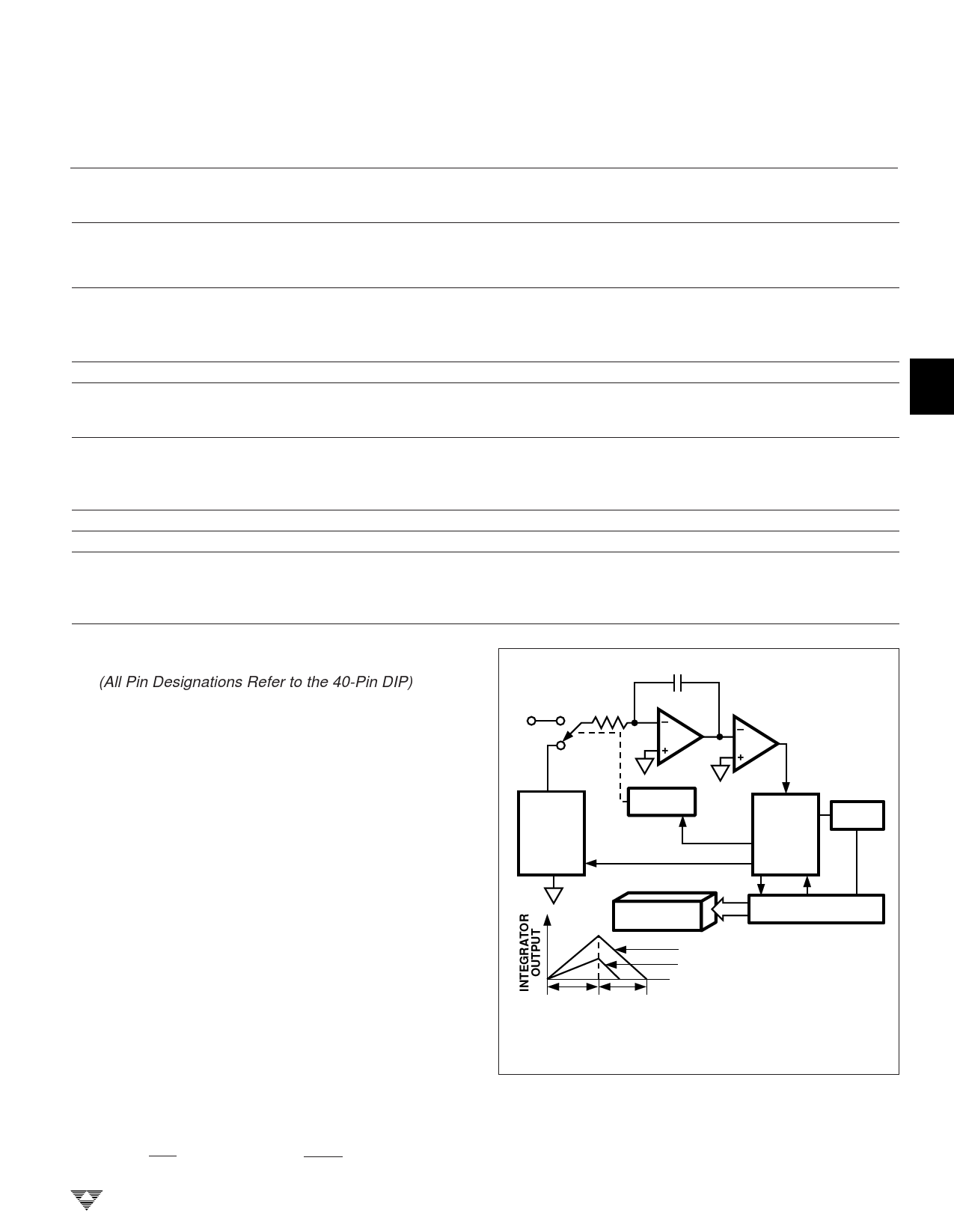
GENERAL THEORY OF OPERATION
(All Pin Designations Refer to the 40-Pin DIP)
Dual-Slope Conversion Principles
The TC7126A is a dual-slope, integrating analog-to-
digital converter. An understanding of the dual-slope con-
version technique will aid in following detailed TC7126A
operational theory.
The conventional dual-slope converter measurement
cycle has two distinct phases:
(1) Input signal integration
(2) Reference voltage integration (deintegration)
The input signal being converted is integrated for a
fixed time period (tSI), measured by counting clock pulses.
An opposite polarity constant reference voltage is then
integrated until the integrator output voltage returns to
zero. The reference integration time is directly proportional
to the input signal (tRI).
In a simple dual-slope converter, a complete conver-
sion requires the integrator output to "ramp-up" and "ramp-
down."
A simple mathematical equation relates the input signal,
reference voltage, and integration time:
∫ 1
tSI VIN(t) dt = VR tRI ,
RC 0
RC
TELCOM SEMICONDUCTOR, INC.
ANALOG
INPUT
SIGNAL
INTEGRATOR
–
+
COMPARATOR
–
+
REF
VOLTAGE
SWITCH
DRIVER
PHASE
CONTROL
CONTROL
LOGIC
POLARITY CONTROL
CLOCK
5
6
DISPLAY
COUNTER
VIN Ϸ VFULL SCALE
VIN Ϸ 1.2 VFULL SCALE
FIXED
SIGNAL
INTEGRATE
TIME
VARIABLE
REFERENCE
INTEGRATE
TIME
7
Figure 1. Basic Dual-Slope Converter
where:
VR = Reference voltage
tSI = Signal integration time (fixed)
8
tRI = Reference voltage integration time (variable).
3-221
Share Link: 