TC7129 View Datasheet(PDF) - TelCom Semiconductor Inc => Microchip
Part Name
Description
Manufacturer
TC7129
TelCom Semiconductor Inc => Microchip

TC7129 Datasheet PDF : 15 Pages
| |||
4-1/2 DIGIT ANALOG-TO-DIGITAL
CONVERTER WITH ON-CHIP LCD DRIVERS
TC7129
ABSOLUTE MAXIMUM RATINGS*
Supply Voltage (V+ to V–) ............................................ 15V
Reference Voltage (REF HI or REF LO) .............. V+ to V–
Input Voltage (IN HI or IN LO) (Note 1) ................ V+ to V–
VDISP ................................................V+ to (DGND – 0.3V)
Digital Input, Pins
1, 2, 19, 20, 21, 22, 27, 37, 39, 40 .......... DGND to V+
Analog Input, Pins 25, 29, 30 ............................... V+ to V–
Package Power Dissipation (TA ≤ 70°C)
Plastic DIP ........................................................1.23W
PLCC ................................................................1.23W
Plastic QFP .......................................................1.00W
Operating Temperature Range .................... 0°C to +70°C
Storage Temperature Range ................ – 65°C to +150°C
Lead Temperature (Soldering, 10 sec) ................. +300°C
Notes: Input voltages may exceed supply voltages, provided input current
is limited to ±400 µA. Currents above this value may result in invalid display
readings but will not destroy the device if limited to ±1 mA.
Dissipation ratings assume device is mounted with all leads soldered to
printed circuit board.
*Static-sensitive device. Unused devices must be stored in conductive
material. Protect devices from static discharge and static fields. Stresses
above those listed under Absolute Maximum Ratings may cause perma-
nent damage to the device. These are stress ratings only and functional
operation of the device at these or any other conditions above those
indicated in the operational sections of the specifications is not implied.
Exposure to Absolute Maximum Rating Conditions for extended periods
may affect device reliability.
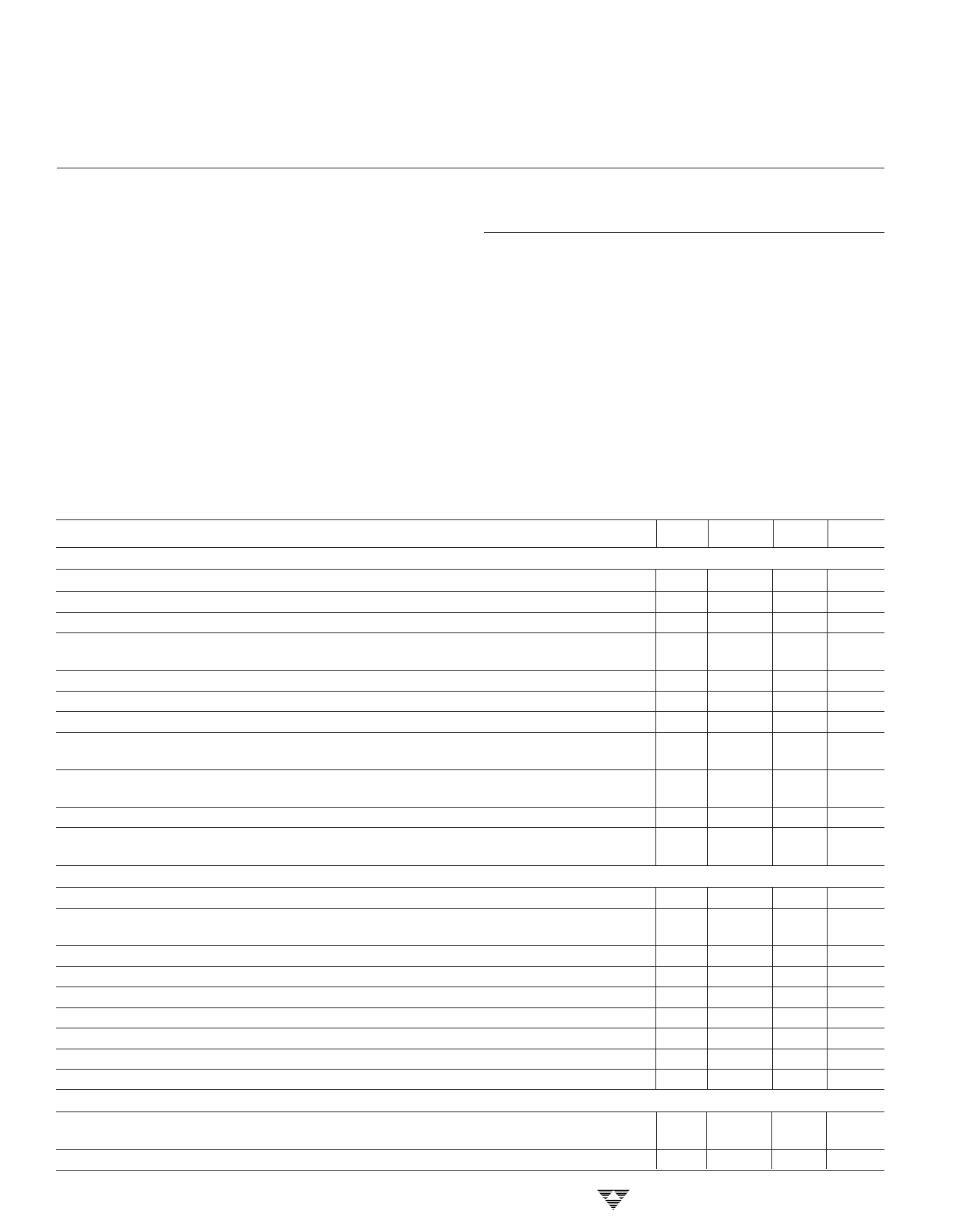
ELECTRICAL CHARACTERISTICS: V+ to V– = 9V, VREF = 1V, TA = +25°C, fCLK = 120 kHz, unless otherwise
indicated. Pin numbers refer to 40-pin DIP.
Symbol Parameter
Test Conditions
Min Typ Max Unit
Input
RE
NL
CMRR
CMVR
eN
IIN
Power
VCOM
DGND
IS
fCLK
Digital
Zero Input Reading
Zero Reading Drift
Ratiometric Reading
Range Change Accuracy
Roll-Over Error
Linearity Error
Common-Mode Rejection Ratio
Common-Mode Voltage Range
Noise (Peak-to-Peak Value Not
Exceeded 95% of Time)
Input Leakage Current
Scale Factor Temperature
Coefficient
Common Voltage
Common Sink Current
Common Source Current
Digital Ground Voltage
Sink Current
Supply Voltage Range
Supply Current Excluding Common Current
Clock Frequency
VDISP Resistance
Low-Battery Flag Activation Voltage
VIN = 0V, 200 mV Scale
VIN = 0V, 0°C < TA < +70°C
VIN = VREF = 1000 mV, Range = 2V
VIN = 0.1V on Low Range
ϬVIN = 1V on High Range
–VIN = +VIN = 199 mV
200 mV Scale
VCM = 1V, VIN = 0V, 200 mV Scale
VIN = 0V
200 mV Scale
VIN = 0V
200 mV Scale
VIN = 0V, Pins 32, 33
VIN = 199 mV, 0°C < TA < +70°C
External VREF = 0 ppm/°C
– 0000 0000
—
±0.5
9997 9999
0.9999 1.0000
+0000 Counts
— µV/°C
10000 Counts
1.0001 Ratio
—
1
2 Counts
—
1
— Counts
—
110
— dB
— (V–) +1.5 — V
— (V+) –1 — V
—
14
— µVP-P
—
1
—
2
10 pA
7 ppm/°C
V+ to Pin 28
∆Common = +0.1V
∆Common = –0.1V
V+ to Pin 36, V+ to V– = 9V
∆DGND = +0.5V
V+ to V–
V+ to V– = 9V
VDISP to V+
V+ to V–
2.8
3.2
—
0.6
—
10
4.5
5.3
—
1.2
6
9
—
0.8
—
120
—
50
6.3
7.2
3.5
V
—
mA
—
µA
5.8
V
—
mA
12
V
1.3 mA
360 kHz
—
kΩ
7.7
V
Continuity Comparator
Threshold Voltages
Pull-Down Current
VOUT Pin 27 = High
VOUT Pin 27 = Low
Pins 37, 38, 39
100 200
—
200
—
2
—
mV
400 mV
10
µA
3-232
TELCOM SEMICONDUCTOR, INC.
Share Link: