TC7107ACKW View Datasheet(PDF) - Microchip Technology
Part Name
Description
Manufacturer
TC7107ACKW Datasheet PDF : 34 Pages
| |||
TC7106/A/TC7107/A
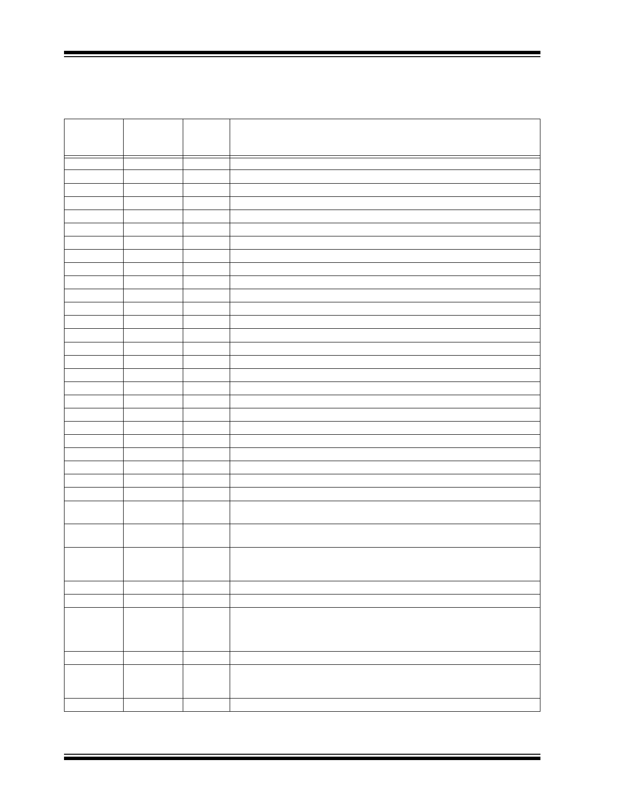
2.0 PIN DESCRIPTIONS
The descriptions of the pins are listed in Table 2-1.
TABLE 2-1: PIN FUNCTION TABLE
Pin Number
Pin No.
(40-Pin PDIP) (40-Pin PDIP)
Normal
(Reversed
Symbol
Description
1
(40)
V+
Positive supply voltage.
2
(39)
D1
Activates the D section of the units display.
3
(38)
C1
Activates the C section of the units display.
4
(37)
B1
Activates the B section of the units display.
5
(36)
A1
Activates the A section of the units display.
6
(35)
F1
Activates the F section of the units display.
7
(34)
G1
Activates the G section of the units display.
8
(33)
E1
Activates the E section of the units display.
9
(32)
D2
Activates the D section of the tens display.
10
(31)
C2
Activates the C section of the tens display.
11
(30)
B2
Activates the B section of the tens display.
12
(29)
A2
Activates the A section of the tens display.
13
(28)
F2
Activates the F section of the tens display.
14
(27)
E2
Activates the E section of the tens display.
15
(26)
D3
Activates the D section of the hundreds display.
16
(25)
B3
Activates the B section of the hundreds display.
17
(24)
F3
Activates the F section of the hundreds display.
18
(23)
E3
Activates the E section of the hundreds display.
19
(22)
AB4 Activates both halves of the 1 in the thousands display.
20
(21)
POL Activates the negative polarity display.
21
(20)
BP/GND LCD Backplane drive output (TC7106A). Digital Ground (TC7107A).
22
(19)
G3
Activates the G section of the hundreds display.
23
(18)
A3
Activates the A section of the hundreds display.
24
(17)
C3
Activates the C section of the hundreds display.
25
(16)
G2
Activates the G section of the tens display.
26
(15)
V-
Negative power supply voltage.
27
(14)
VINT Integrator output. Connection point for integration capacitor. See INTEGRATING
CAPACITOR section for more details.
28
(13)
VBUFF Integration resistor connection. Use a 47 kΩ resistor for a 200 mV full scale range
and a 47 kΩ resistor for 2V full scale range.
29
(12)
CAZ The size of the auto-zero capacitor influences system noise. Use a 0.47 µF capacitor
for 200 mV full scale, and a 0.047 µF capacitor for 2V full scale. See Section 7.1
“Auto-Zero Capacitor (CAZ)” on Auto-Zero Capacitor for more details.
30
(11)
VIN- The analog LOW input is connected to this pin.
31
(10)
VIN+ The analog HIGH input signal is connected to this pin.
32
(9)
ANALOG This pin is primarily used to set the Analog Common mode voltage for battery
COMMON operation or in systems where the input signal is referenced to the power supply. It
also acts as a reference voltage source. See Section 8.3 “Analog Common (Pin
32)” on ANALOG COMMON for more details.
33
(8)
CREF- See Pin 34.
34
(7)
CREF+ A 0.1 µF capacitor is used in most applications. If a large Common mode voltage
exists (for example, the VIN- pin is not at analog common), and a 200 mV scale is
used, a 1 µF capacitor is recommended and will hold the rollover error to 0.5 count.
35
(6)
VREF- See Pin 36.
DS21455D-page 6
© 2008 Microchip Technology Inc.
Share Link: 