TC7129(2002) View Datasheet(PDF) - Microchip Technology
Part Name
Description
Manufacturer
TC7129
(Rev.:2002)
(Rev.:2002)
Microchip Technology

TC7129 Datasheet PDF : 24 Pages
| |||
TC7129
4.5 +5V Power Supply
Measurements are made with respect to power supply
ground. COMMON (Pin 28) is connected to REF LO
(Pin 35). A voltage doubler is needed, since the supply
voltage is less than the 6V minimum needed by the
TC7129. DGND (Pin 36) must be isolated from power
supply ground (see Figure 4-3).
FIGURE 4-3:
+5V
POWERING THE TC7129
FROM A +5V POWER
SUPPLY
0.1µF
24
V+
34
TC7129
35
36 DGND
28
0.1µF
33
+
8
V+
2
VIN
32
V-
–
+
23
TC7660 4
10µF
GND
3
5
10µF
+
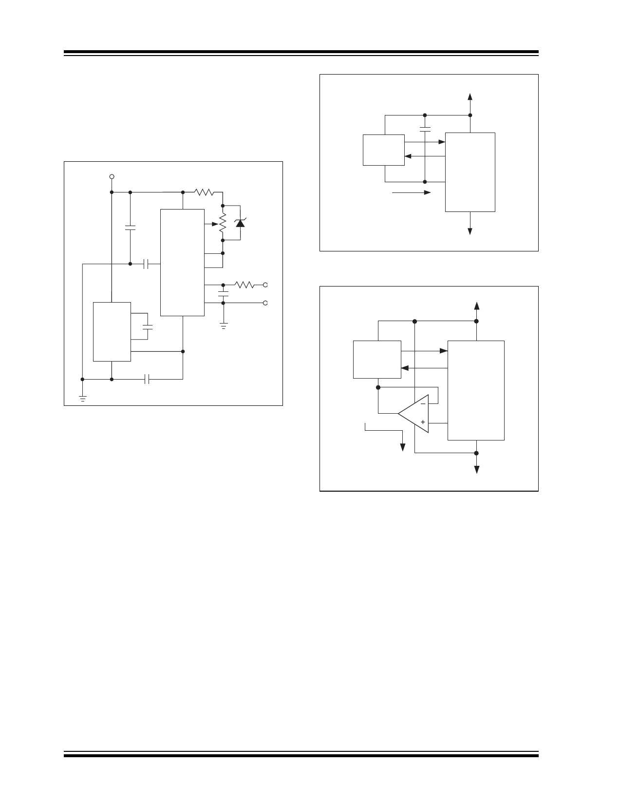
4.6 Connecting to External Logic
External logic can be directly referenced to DGND
(Pin 36), provided that the supply current of the exter-
nal logic does not exceed the sink current of DGND
(Figure 4-4). A safe value for DGND sink current is
1.2mA. If the sink current is expected to exceed this
value, a buffer is recommended (see Figure 4-5).
FIGURE 4-4:
EXTERNAL LOGIC
REFERENCED DIRECTLY
TO DGND
V+
External
Logic
ILOGIC
24
TC7129
36
DGND
23
V-
FIGURE 4-5:
EXTERNAL LOGIC
REFERENCED TO DGND
WITH BUFFER
V+
External
Logic
24
TC7129
ILOGIC
36
DGND
23
V-
4.7 Temperature Compensation
For most applications, VDISP (Pin 19) can be connected
directly to DGND (Pin 36). For applications with a wide
temperature range, some LCDs require that the drive
levels vary with temperature to maintain good viewing
angle and display contrast. Figure 4-6 shows two cir-
cuits that can be adjusted to give temperature com-
pensation of about 10mV/°C between V+ (Pin 24) and
VDISP. The diode between DGND and VDISP should
have a low turn-on voltage because VDISP cannot
exceed 0.3V below DGND.
DS21459B-page 10
© 2002 Microchip Technology Inc.
Share Link: