TD7104FG View Datasheet(PDF) - Toshiba
Part Name
Description
Manufacturer
TD7104FG Datasheet PDF : 6 Pages
| |||
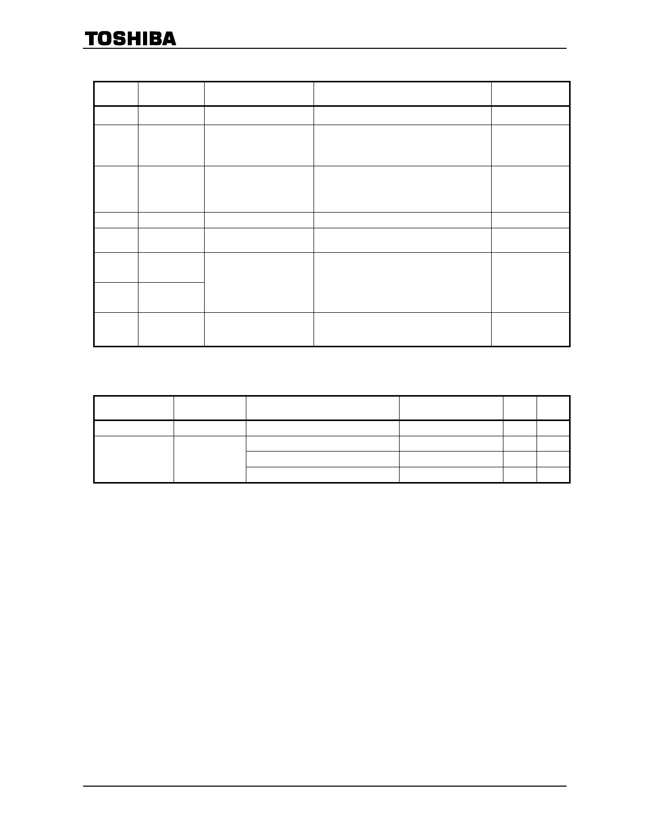
Pin Function
Pin No.
1
Symbol
VCC
2
FMIN
Pin Name
Power supply terminal
FM local OSC. signal
input terminal
3
TVIN
TV local OSC. signal
input terminal
4
GND
Ground terminal
5
Out
Dividing signal output
terminal
6
N1
Dividing ratio selecting
control terminal
7
N2
8
BIAS
BIAS terminal
TD7104FG
Function And Description
Remarks
Applies voltage of VCC = 3.0 to 5.5V
―
Inputs local oscillation signal in FM band.
fIN = 50 to 200MHz, FMIN input signal is
output by a 1 / 1 dividing ratio (buffer amplifier).
Built−in input
Amp. provided
Inputs local oscillation signal in TV band.
FIN = 50M to 1.0GHz, TVIN input signal is
output by a 1 / 8, 1 / 4, or 1 / 2 dividing ratio,
which is controlled through N1 and N2 input.
Grounds.
Built−in input
Amp. provided
―
Outputs dividing signal.
―
These inputs control the selection of a
dividing ratio among 1 / 1, 1 / 2, 1 / 4, and
1 / 8.
FMIN terminal is selected at N1 = N2 = "L"
―
level (1 / 1 dividing).
The truth table is shown below.
Connects capacitors on bias circuit.
Change this pin to low to convert the IC is to
―
stand−by mode.
Truth Table
Receiving Band
FM
Input Terminal
FMIN
TV
TVIN
Operating Frequency Range
50M~200MHz
50M~400MHz
100M~500MHz
100M~1.0GHz
Dividing Ratio
÷1
÷2
÷4
÷8
N1
N2
0
0
1
0
0
1
1
1
2
2004-08-06
Share Link: 