TDA7376PD View Datasheet(PDF) - STMicroelectronics
Part Name
Description
Manufacturer
TDA7376PD Datasheet PDF : 9 Pages
| |||

TDA7376PD
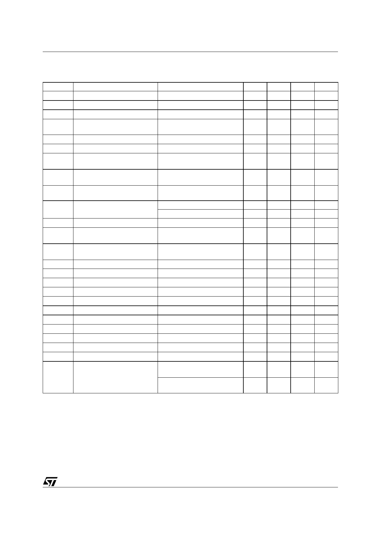
ELECTRICAL CHARACTERISTCS (Refer to the test circuits figgs 1 and 2, VS = 14.4V; RL = 4Ω; f = 1KHz;
Tamb = 25°C, unless otherwise specified).
Symbol
Parameter
Test Condition
Min. Typ. Max. Unit
VS
Supply Voltage Range
8
18
V
Id
Total Quiescent Drain Current RL = ∞
200
mA
VOS Output Offset Voltage
120
mV
PO
Output Power
THD = 10%;
23
25
W
THD = 10%; RL = 2Ω
33
37
W
PO max Max. Output Power (*)
36
40
W
PO EIAJ EIAJ Outout Power (*)
VS = 13.7V
32
35
W
THD Distortion
PO = 0.5 to 10W
PO = 0.5 to 15W
0.03
%
0.08
%
CT
Cross Talk
f = 1KHz; Rg
f = 10KHz; Rg
80
dB
70
dB
RIN
Input Impedance
differential input
45
KΩ
Single Ended input
40
KΩ
GV
Voltage Gain
differential input
Single Ended input
25
26
27
dB
25
26
27
dB
∆GV Channel Gain Balance
1
dB
EIN Input Noise Voltage
Rg = 600Ω; "A" weighted
Rg = 600Ω; 22Hz to 33KHz
3
µV
4
6
µV
SVR Supply Voltage Rejection
f = 100Hz; Vr = 1Vrms; Rg = 0;
45
dB
f = 10Hz; Vr = 1Vrms; Rg = 0;
55
dB
BW Power Bandwidth
(-3dB)
75
kHz
CMRR Common Mode Rejection Ratio VCM = 1Vrms input referred
60
dB
ASB Stand-by Attenuation
VSB = 1.5V; PO ref = 1W
80
90
dB
VSB IN Stand-by In Threshold
1.5
V
VSB OUT Stand-by Out Threshold
3.5
V
Isb
Stand-by Current Consumption VSB = 0V
20
µA
AM
Mute Attenuation
VM = 1.5V; POref = 1W
85
dB
VM IN Mute in Threshold
1.5
V
VM OUT Mute out Threshold
3.5
V
I6
Mute pin Current
V6 = 0 to VS, ; VS max. = 18V
100
µA
DDL Distortion Detection Level (**)
3.5
%
DDOUT Distortion Detector Output DC Output low, sinked current
1
mA
Current
(Vpin10 = 1.5V)
Output high, leakage current
(Vpin10 = VS, @ VSmax = 18V)
10
µA
(*) Saturated square wave output
(**) see figure 5 for THD setting.
The TDA7376PD is equipped with a programmable clipping distortion detector circuitry that allows to sig-
nal out the output stage saturation by providing a current sinking into an open collector output (DDout)
when the total harmonic distortion of the output signal reaches the preset level. The desired threshold is
fixed through an external divider that produces a proper voltage level across the THD set pin. Fig. 4 shows
the THD detection threshold versus the THD set voltage. Since it is essential that the THD set voltage be
proportional to the supply voltage, fig. 5 shows its value as a fraction of VCC. The actual voltage can be
computed by multiplying the fraction corresponding to the desired THD threshold by the application’s sup-
ply voltage.
5/9